Light-emitting diode (LED) epitaxial layer structure and LED chip with same

A technology of epitaxial layer and structural unit, which is applied in the direction of electrical components, circuits, semiconductor devices, etc., can solve problems such as MQW layer damage, and achieve the effects of improving bonding efficiency, improving mobility, and increasing recombination efficiency

Inactive Publication Date: 2014-08-06
XIANGNENG HUALEI OPTOELECTRONICS
View PDF4 Cites 19 Cited by
  • Summary
  • Abstract
  • Description
  • Claims
  • Application Information

AI Technical Summary

Problems solved by technology

[0004] The purpose of the present invention is to provide an LED epitaxial layer structure and an LED chip with the structure to solve the problem that the P-type GaN layer in the prior art cannot effectively block some electrons from entering the hole injection layer to form a non-radiative recombination and high-temperature P-type GaN layer. Technical issues of growth conditions causing damage to the MQW layer

Method used


Image

  • Light-emitting diode (LED) epitaxial layer structure and LED chip with same
  • Light-emitting diode (LED) epitaxial layer structure and LED chip with same
  • Light-emitting diode (LED) epitaxial layer structure and LED chip with same

Examples


preparation example Construction

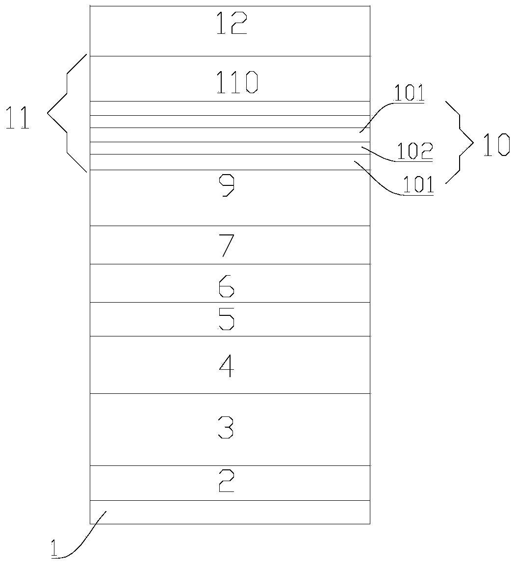
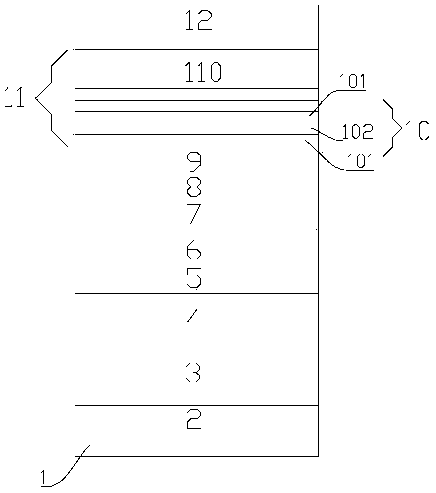
[0049] The LED epitaxial layer preparation method provided by the present invention comprises the following steps:

[0050] The following growth processes are carried out in MOCVD equipment by MOCVD method.

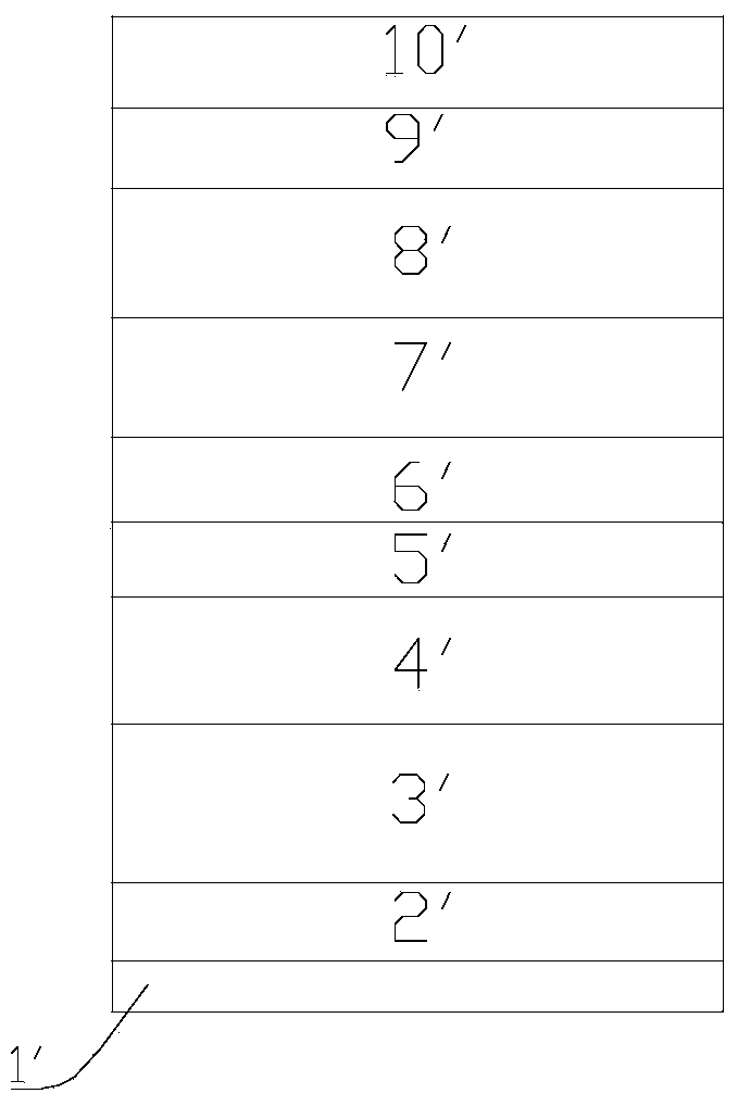
[0051] 1. Place the sapphire substrate 1 in the MOCVD reaction chamber, and use H 2 , NH 3 Wait for the gas to treat the sapphire substrate 1 for 4 to 10 minutes;

[0052] 2. After the treatment is completed, the temperature of the reaction chamber is lowered to 500-650°C, the optimum temperature is 550°C, and TMGa and NH 3 , the pressure is 300-900mbar, and a GaN buffer layer 2 (Nucleation) with a thickness of 20-50nm is grown on the sapphire substrate 1;

[0053] 3. After the GaN buffer layer 2 is grown, the temperature is raised to 950-1100° C., annealed for 60-300 s, and a GaN crystal nucleus is formed on the substrate 1;

[0054] 4. After the annealing is completed, the temperature is adjusted to 950-1050°C, and TMGa and NH 3 , with a pressure of 300-900mbar, gr...

Embodiment 1

[0070] 1. Place the sapphire substrate 1 in the MOCVD reaction chamber, at a temperature of 1000°C, use H 2 , NH 3 Wait for gas treatment for 4 minutes for sapphire substrate 1;

[0071] 2. After the treatment is completed, the temperature of the reaction chamber is lowered to within 500°C, and TMGa and NH are introduced 3 , the pressure is 300mbar, and a GaN buffer layer 2 (Nucleation) with a thickness of 20nm is grown on the sapphire substrate 1;

[0072] 3. After growing the GaN buffer layer 2, raise the temperature to 950°C and anneal for 60s to form a GaN crystal nucleus on the substrate 1;

[0073] 4. After the annealing is completed, the temperature is adjusted to 950°C, and TMGa and NH are introduced 3 , the pressure is 300mbar, and the first u-GaN layer 3 with a thickness of 0.8um is grown on the GaN buffer layer 2;

[0074] 5. Then raise the temperature to 1000° C. and the pressure to 300 mbar, and grow the second u-GaN layer 4 with a thickness of 2 μm.

[0075]...

Embodiment 2

[0085] 1. Place the sapphire substrate 1 in the MOCVD reaction chamber, at a temperature of 1100°C, use H 2 , NH 3 Wait for the gas to treat the sapphire substrate 1 for 10 minutes;

[0086] 2. After the treatment is completed, the temperature of the reaction chamber is lowered to within 650°C, and TMGa and NH are introduced 3 , the pressure is 900mbar, and a GaN buffer layer 2 (Nucleation) with a thickness of 50nm is grown on the sapphire substrate 1;

[0087] 3. After growing the GaN buffer layer 2, raise the temperature to 1100°C and anneal for 300s to form a GaN crystal nucleus on the substrate 1;

[0088] 4. After the annealing is completed, the temperature is adjusted to 1050°C, and TMGa and NH are introduced 3 , the pressure is 900mbar, and the first u-GaN layer 3 with a thickness of 1.5um is grown on the GaN buffer layer 2;

[0089] 5. The temperature is raised to 1100° C., the pressure is 900 mbar, and the second u-GaN layer 4 with a thickness of 3 μm is grown.

...


PUM


Abstract

The invention provides a light-emitting diode (LED) epitaxial layer structure and an LED chip with the same. The epitaxial layer structure comprises an MQW layer, an electronic barrier layer and a P-type GaN hole injection layer, which sequentially grow, wherein the P-type GaN hole injection layer comprises a hole injection layer and also a P-type AlGaN / GaN superlattice layer growing between the electronic barrier layer and the hole injection layer. According to the LED epitaxial layer structure provided by the invention, an MQW protective layer is arranged between the electronic barrier layer and the MQW layer, and then the P-type AlGaN / GaN superlattice layer is arranged on the electronic barrier layer, so that even diffusion of the hole is facilitated by a two-dimensional carrier gas formed by the P-type AlGaN / GaN superlattice layer, and the joint efficiency between electronics and holes is improved.

Description

technical field [0001] The invention relates to the field of LED (Light Emitting Diode), in particular to an LED epitaxial layer structure and an LED chip with the structure. Background technique [0002] The GaN semiconductor material with wide bandgap has good chemical stability, thermal stability and high breakdown voltage. It is the third-generation new semiconductor material after the first-generation silicon material and the second-generation gallium arsenide material. The bandgap of its ternary alloy Indium Gallium Nitride (InXGa1-XN) is continuously adjustable from 0.7eV to 3.4eV, and the emission wavelength covers the visible and near-ultraviolet regions. It is considered to be an ideal material for manufacturing high-brightness blue and green light-emitting diodes and white light-emitting diodes, and has been widely used in lighting, display screens, backlight sources, signal lights and other fields. [0003] Such as figure 1 As shown, the traditional GaN-based L...

Claims


Application Information

Patent Timeline
Patent Type & Authority Applications(China)
IPC IPC(8): H01L33/00H01L33/06
CPCH01L33/06H01L33/0066H01L33/0075
Inventor 马欢徐迪田艳红
Owner XIANGNENG HUALEI OPTOELECTRONICS
Why Eureka
Try Eureka