Organic light emitting device and manufacturing method thereof
An electroluminescence device and luminescence technology, which is applied in the direction of electric solid-state devices, semiconductor/solid-state device manufacturing, electrical components, etc., can solve the problems of small material selection range, complicated adjustment of process parameters, complex preparation process, etc., and achieve easy large-scale The effects of area film formation, excellent process repeatability, and simple processing methods
- Summary
- Abstract
- Description
- Claims
- Application Information
AI Technical Summary
Problems solved by technology
Method used
Image
Examples
Embodiment 1
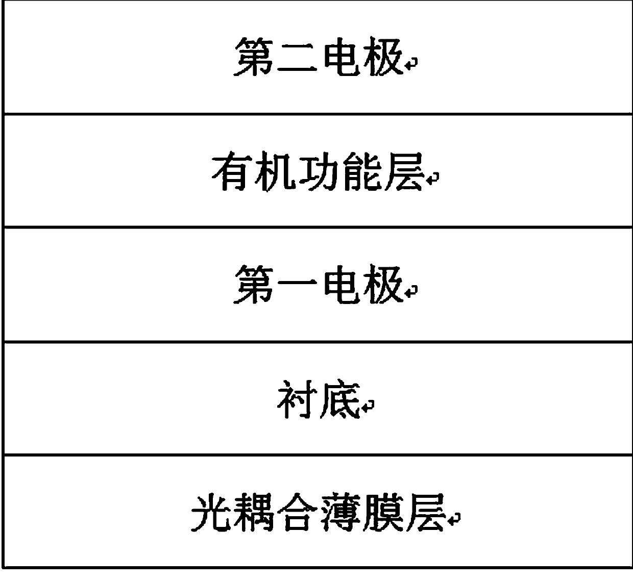
[0055] An organic electroluminescence device, such as figure 1 As shown, a transparent substrate, a first electrode arranged on one side of the transparent substrate and stacked in sequence, an organic functional layer and a second electrode, and an optical coupling thin film layer arranged on the other side of the transparent substrate are provided.
[0056] The optical coupling film layer is provided with a layer body and a patterned layer arranged on the surface of the layer body. The visible light transmittance of the optical coupling film layer is greater than 60%, the refractive index is greater than 1.6, and the thickness of the optical coupling film layer is 1-1000 microns.
[0057] The layer body of the optical coupling film layer is a transparent layer body, and its preparation materials can be polymethyl methacrylate (PMMA), polyimide (PI), polydimethylsiloxane (PDMS), polyterephthalene Ethylene glycol formate (PET), epoxy resin (EP), polycarbonate (PC), nylon (PA)...
Embodiment 2
[0063] An organic electroluminescence device, the other features are the same as those in Embodiment 1, except that: the optical coupling film layer is provided with a layer body and micropores distributed inside the layer body or on the surface of the layer body.
[0064] The maximum diameter of the micropores is in the range of 1-200 microns, and the duty ratio of the micropores on the surface of the layer is greater than 0.1. The duty ratio refers to the ratio of the area of the micropores on the surface of the layer to the area of the layer. Since the micropores should not be defined as regular circular holes, the maximum diameter of the micropores here refers to the distance between the two furthest points of the micropores.
[0065] Micropores can include either or both of open and closed cell frameworks. Microwells can be of any suitable shape or size, such as spherical, cylindrical, slit-shaped, and the like. If the micropores are open, the micropores may form mul...
Embodiment 3
[0071] An organic electroluminescent device, the other features are the same as in Embodiment 1, the difference is that the optical coupling film layer is provided with a layer, micropores distributed inside the layer or on the surface of the layer, and a pattern arranged on the surface of the layer layers. When preparing the optical coupling film layer, the microporous structure is prepared first, and then the patterned layer is processed on the surface of the layer body. It has the characteristics of good light extraction effect, simple processing method and good device performance.
PUM
 Abstract
Description
Claims
Application Information


