Non-vacuum method for producing light absorbing material applied in solar battery

A battery and formula technology, applied in the direction of final product manufacturing, sustainable manufacturing/processing, circuits, etc., can solve the problems of increased surface roughness, long time selenization, adverse effects of battery efficiency, etc., and achieve the effect of low manufacturing cost

Active Publication Date: 2014-09-10
NANO & ADVANCED MATERIALS INST
View PDF7 Cites 9 Cited by
  • Summary
  • Abstract
  • Description
  • Claims
  • Application Information

AI Technical Summary

Problems solved by technology

Soft annealing is necessary to avoid the formation of secondary phases (e.g. Cu 2 (S/Se), Cu 2-X (S/Se), Sn(S/Se) 2 , Sn 2 (S/Se) 3 、Cu 2 Sn(S/Se) 3 , Zn(S/Se), etc.), and the secondary phase will eventually adversely affect the efficiency of ...

Method used


Image

  • Non-vacuum method for producing light absorbing material applied in solar battery
  • Non-vacuum method for producing light absorbing material applied in solar battery
  • Non-vacuum method for producing light absorbing material applied in solar battery

Examples


Embodiment approach

[0037] According to an exemplary embodiment of the present invention, preferably control about 3mA / cm 2 to about 10mA / cm 2 current density to deposit the selenium layer. The formulation deposition bath will be heated to a preferred temperature range of 60°C to 120°C. In all cases, the deposition bath temperature should be kept constant during the deposition process.

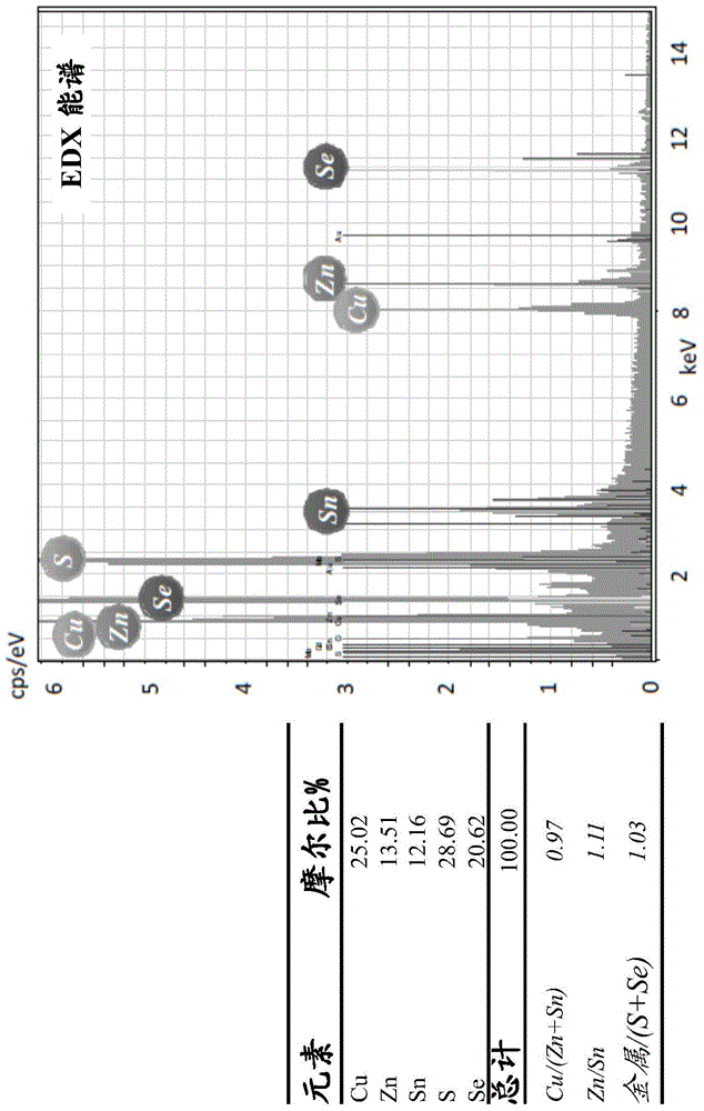
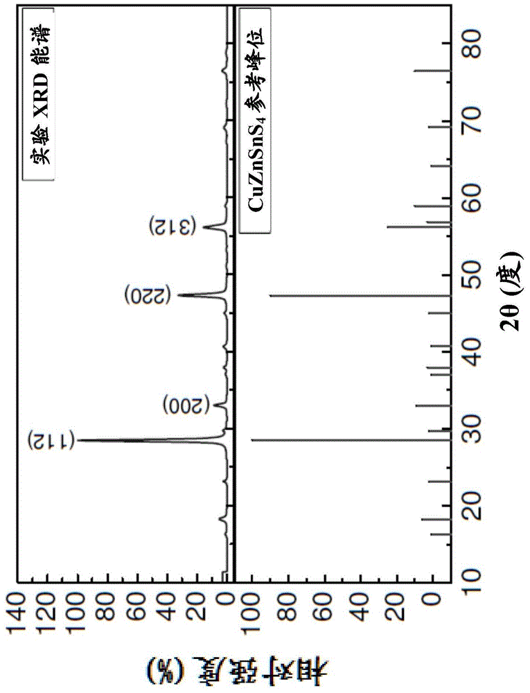
[0038] By using the plating-annealing approach, EDX spectroscopy ( figure 2 ) shows that a CZTS film with an atomic ratio of 2:1:1:4 can be deposited on a conductive substrate, which is the same as the simplest formula of CZTS, that is, Cu 2 ZnSn(S y Se 1-y ) 4 The element ratios are the same. In terms of crystal structure and chemical composition, the obtained CZTS film after annealing shows the same diffraction pattern in the XRD spectrum as the CZTS absorbing layer disclosed in the crystallography database ( image 3 ). These results confirm the feasibility of converting the CZTS precursor stacked la...

Embodiment 1

[0040] Example 1 - Formation of Cu-Zn-Sn alloy by a single deposition bath formulation

[0041] In this example, a Cu-Zn-Sn alloy was prepared by a single deposition bath containing the components of the electroplating recipe. Table 1 provides an exemplary electroplating formulation composition.

[0042] Table 1:

[0043]

[0044]

[0045] In addition to ionic compounds of copper, zinc, and tin, the electroplating composition also contains citrate salts to stabilize the plating bath, and additives to reduce surface roughness, such as surfactants and aldehyde-based compounds. Table 1 lists optimum ranges and examples of each component in the electroplating composition.

[0046] Citrates in the deposition bath formulations in Table 1 can be based on dicarboxylates (e.g. oxalate, malonate, succinate), tricarboxylates (e.g. isocitrate, propane-1,2 ,3-tricarboxylate, benzene-1,3,5-tricarboxylate) and polycarboxylate polymer salt substitution. The substitutes exhibit simil...

Embodiment 2-C

[0048] Sequential sulfurization and selenization of embodiment 2-Cu-Zn-Sn alloy layer

[0049] The annealing step is a necessary process to transform the Cu-Zn-Sn alloy into a CZTS light-absorbing layer. Table 2 illustrates the annealing conditions used for sulfurization and selenization.

[0050] Table 2:

[0051]

[0052]

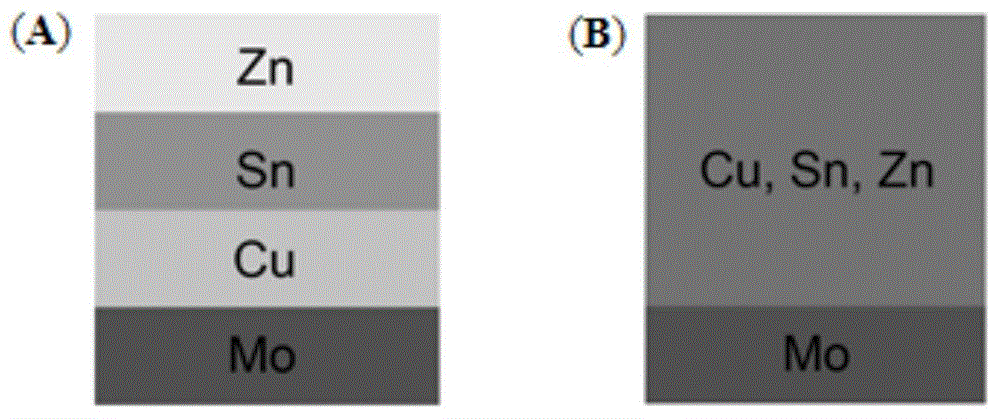
[0053] Figure 4 The flow chart from the formation of Cu-Zn-Sn alloy to annealing is shown: 401: Formation of Cu-Zn-Sn alloy layer by co-plating on molybdenum (Mo) substrate by single deposition bath formulation; 402: Formation of Cu-Zn-Sn alloy layer by using An inert carrier gas flowing above forms a sulfur-rich atmosphere; 403: Cu-Zn-Sn-S alloy is formed after the first anneal; 404: a selenium-rich atmosphere is formed by using an inert carrier gas flowing over selenium; 405: in A Cu-Zn-Sn-S-Se alloy is formed after the secondary annealing. Figure 5 A schematic is shown outlining the sequential sulfurization and selenization on Cu-Zn-Sn allo...


PUM

PropertyMeasurementUnit
Thicknessaaaaaaaaaa

Abstract

The present invention describes a method for producing p-type light absorbing semiconducting copper zinc tin selenide/sulfide (Cu2(ZnxSn2-x)(SySel-y)4) (CZTS for short) through utilizing electrochemical deposition. The p-type light absorbing semiconducting copper zinc tin selenide/sulfide can be used in manufacturing solar battery when combined with an n-type inorganic or organic semiconductor layer. The method comprises using one step of electroplating or a series of deposition to produce low-cost large-are CZTS solar battery without using an expensive and complex deposition technology or highly toxic and highly flammable chemicals in the manufacturing process. According to the method of the present invention, the cost and energy requirement in manufacturing the solar battery are reduced.

Description

[0001] Cross References to Related Applications [0002] This application claims priority to US Provisional Application 61 / 851,407, filed March 7, 2013, the disclosure of which is incorporated herein by reference in its entirety. technical field [0003] The present invention relates to a method of producing a light absorbing material that can be used in solar cells. Specifically, the present invention provides a method of using electrochemical deposition to manufacture copper-zinc-tin-based selenide / sulfide (Cu 2 (Zn x sn 2-x )(S y Se 1-y ) 4 ) (abbreviated as "CZTS") of p-type light-absorbing semiconductors that can be used to fabricate solar cells when combined with n-type inorganic or organic semiconductor layers. The invention also relates to a light-absorbing semiconductor produced by the method of the invention. Background technique [0004] a-Si, CdTe, and CIGS solar cells are being researched worldwide as next-generation thin-film solar cells following c-Si s...

Claims


Application Information

Patent Timeline
IPC IPC(8): C25D3/56C25D3/58C25D3/60C25D3/38C25D3/22C25D3/30C25D5/10C25D5/50H01L31/032H01L31/18
CPCY02P70/50
Inventor 何锦镖何国强廖敏璍王然石陆伟俊蔡颖豪郑富林郭广宙许美美刘家裕
Owner NANO & ADVANCED MATERIALS INST
Why Eureka
Try Eureka