Super-junction device and manufacturing method thereof

A super junction and device technology, applied in semiconductor/solid-state device manufacturing, semiconductor devices, electrical components, etc., can solve the inability to realize the alternate arrangement structure of P-type semiconductor thin layers and N-type semiconductor thin layers, increase the etching process and silicon Filling process difficulty, increased specific on-resistance, etc., to achieve the effect of low specific on-resistance, reduced process cost, and increased breakdown voltage

CN104037206AActive Publication Date: 2014-09-10SHANGHAI HUAHONG GRACE SEMICON MFG CORP
5 Cites 4 Cited by

Patent Information

Authority / Receiving Office
CN · China
Patent Type
Applications(China)
Current Assignee / Owner
Publication Date
2014-09-10

Smart Images

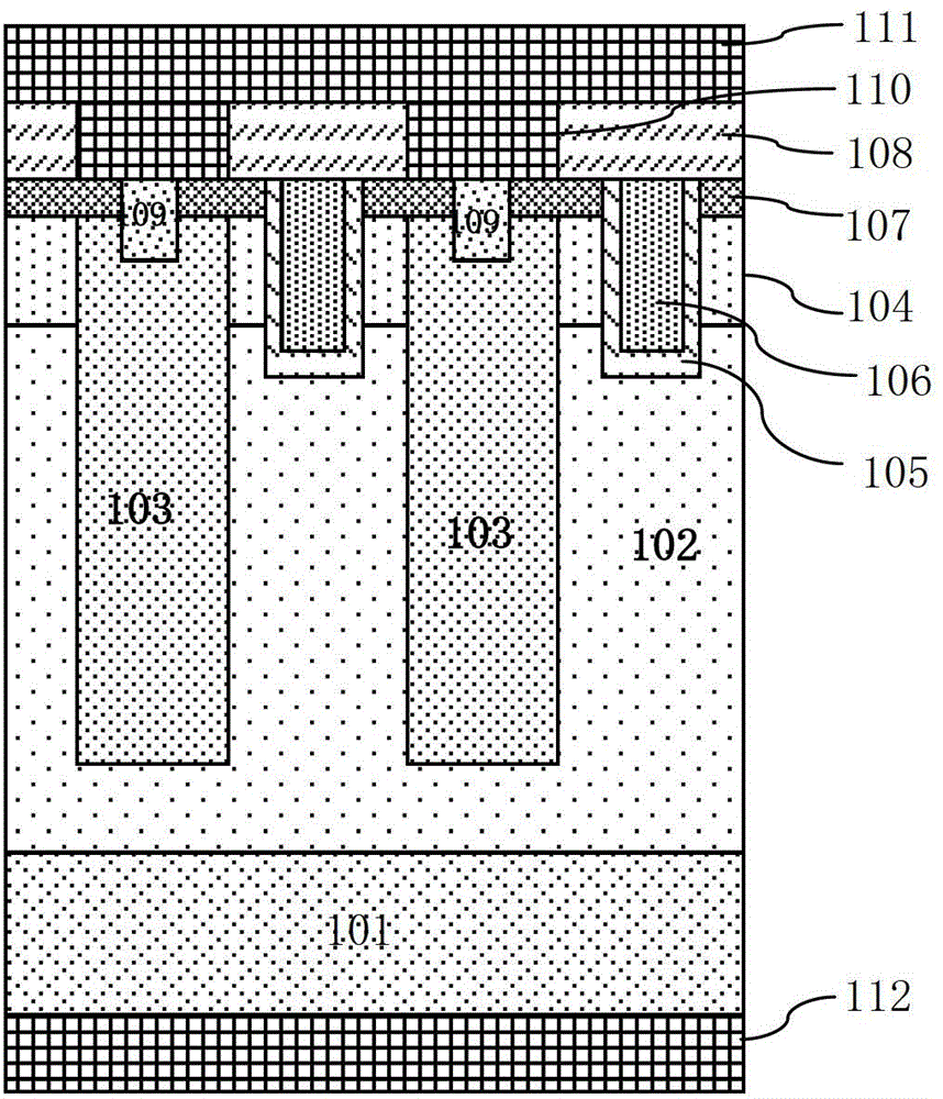
  • Figure 1
    Figure 1
  • Figure 2
    Figure 2
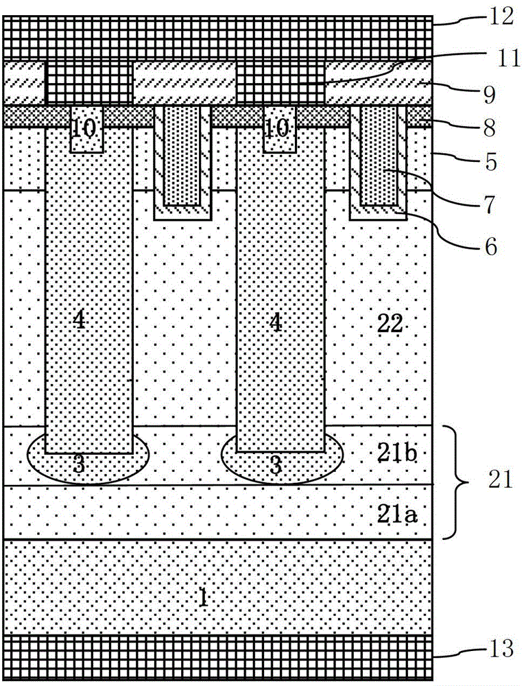
  • Figure 3
    Figure 3
Patent Text Reader

Abstract

The invention discloses a super-junction device. A P type semiconductor thin layer is divided into two layers; one layer at the bottom is formed by a P type ion implantation zone; and the other layer at the top is formed by P type silicon filling a deep trench. The depth of the whole P type thin layer is decided by the longitudinal distance between the bottom surface of the bottom layer and the top surface of the top layer, thereby eliminating the influence on the depth of the P type thin layer by the depth change of the deep trench, realizing precise controlling of the depth of the P type thin layer and improving uniformity of the depth, and enhancing the breakdown voltage of the device. The depth changing range of the deep trench is determined by the depth the P type ion implantation zone of the bottom layer, thereby substantially expanding the process window of the deep trench, reducing the complexity of the process and the process cost, and meeting the requirement of continuous improvement of the carrier concentration of the P type semiconductor thin layer and the N type semiconductor thin layer. The N type epitaxial layer with high concentration can be used and a super-junction device with lower-ratio on resistance can be obtained. In addition, the invention also discloses a manufacturing method of the super-junction device.
Need to check novelty before this filing date? Find Prior Art

Description

technical field

[0001] The invention relates to the field of semiconductor integrated circuit manufacturing, in particular to a super junction device; the invention also relates to a manufacturing method of the super junction device. Background technique

[0002] The super-junction device adopts a new withstand voltage layer structure, that is, a series of alternately arranged P-type and N-type semiconductor thin layers are used to make P-type and N-type semiconductor thin layers composed of P-type and N-type semiconductor thin layers in the off state at a lower voltage. The N-type region is depleted to achieve mutual compensation of charges, so that the P-type N-type region can achieve high breakdown voltage under high doping concentration, thereby obtaining low on-resistance and high breakdown voltage at the same time, breaking the traditional power device theory limit.

[0003] MOSFET (Metal-Oxide-Semiconductor-Field-Effect Transistor) devices with a super-junction struc...

Examples

Embodiment Construction

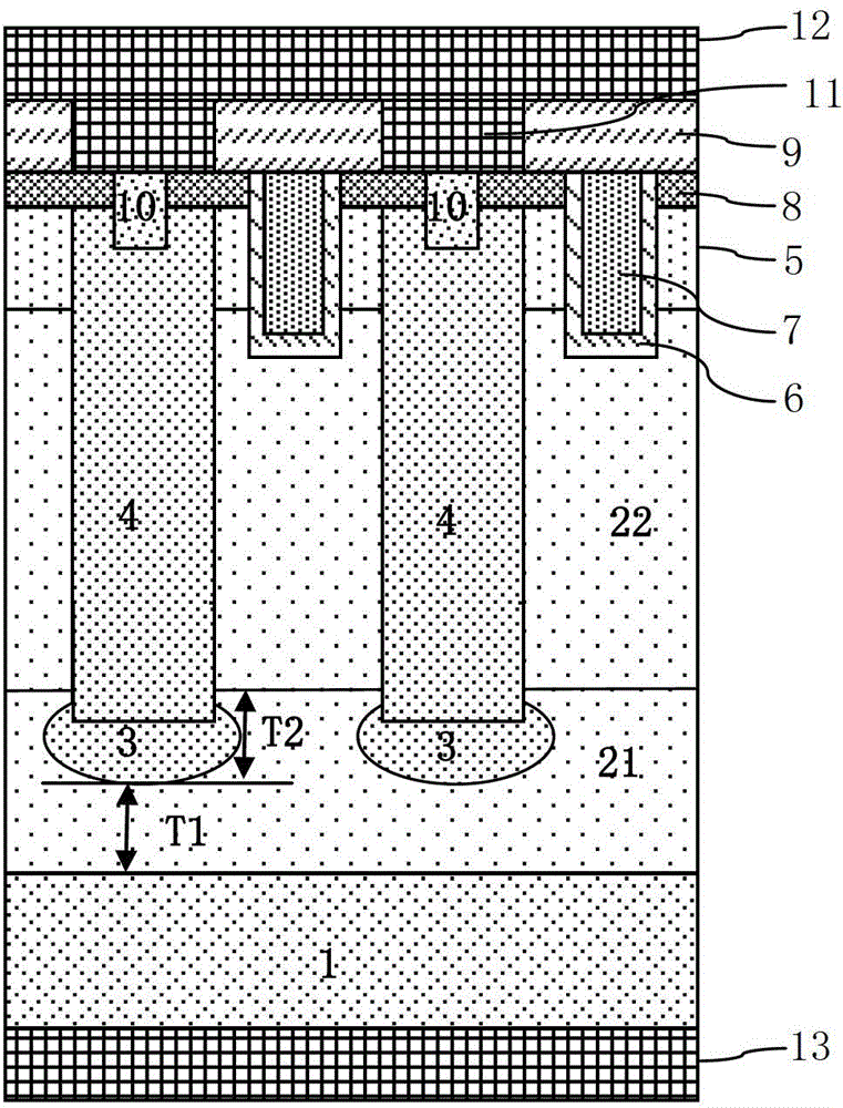
[0035] figure 2 It is a schematic diagram of a super-junction device according to an embodiment of the present invention; a super-junction device according to an embodiment of the present invention is a super-junction NMOSFET device with a breakdown voltage of 600V, and a super-junction device according to an embodiment of the present invention includes:

[0036] On the N+ substrate 1, the substrate 1 is a silicon substrate. The resistivity of the substrate 1 is 0.001 ohm·cm to 0.003 ohm·cm.

[0037] An N-type epitaxial layer is formed on the substrate 1 . The N-type epitaxial layer is composed of a first N-type epitaxial layer 21 and a second N-type epitaxial layer 22 sequentially formed on the substrate 1 . The first N-type epitaxial layer 21 is uniformly doped, such as a doping concentration of 1 ohm·cm; the doping concentration of the second N-type epitaxial layer 22 is also 1 ohm·cm, and the first N-type epitaxial The thickness of the layer 21 is 15 microns, and the t...