Organic light emitting diode and preparation method thereof

An electroluminescent device, organic technology, applied in the direction of electric solid device, semiconductor/solid state device manufacturing, electrical components, etc., can solve the problem of low lumen efficiency, achieve lower interface contact barrier, high lumen efficiency, interface barrier reduced effect

Inactive Publication Date: 2014-09-10
OCEANS KING LIGHTING SCI&TECH CO LTD +2
View PDF4 Cites 7 Cited by
  • Summary
  • Abstract
  • Description
  • Claims
  • Application Information

AI Technical Summary

Problems solved by technology

Electrons and holes meet, recombine, and form excitons in the light-emitting layer. Excitons migrate under the action of an electric field, transfer energy to the light-emitting material, and excite electrons to transition from the ground state to the excited state. The excited state energy is deactivated by radiation to generate photons , to release light energy, but the OLEDs currently researched still generally have the problem of low lumen efficiency

Method used


Image

  • Organic light emitting diode and preparation method thereof
  • Organic light emitting diode and preparation method thereof
  • Organic light emitting diode and preparation method thereof

Examples


preparation example Construction

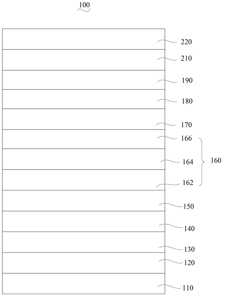
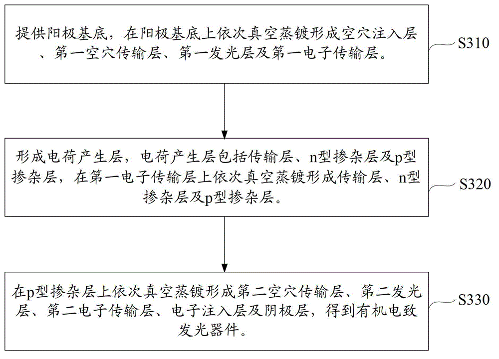
[0045] Such as figure 2 Shown, the preparation method of the organic electroluminescent device of one embodiment, comprises the following steps:

[0046] Step S310: providing an anode substrate, and sequentially vacuum-evaporating a hole injection layer, a first hole transport layer, a first light-emitting layer, and a first electron transport layer on the anode substrate.

[0047] Preferably, before the hole injection layer is formed by vacuum evaporation on the anode substrate, the step of sequentially performing photolithography, cutting and cleaning on the anode substrate is also included. The cleaning step is: ultrasonically clean the cut anode base in detergent, deionized water, propanol, ethanol and isopropanone in sequence, so as to remove organic pollutants on the anode base. Preferably, the time for each ultrasonic cleaning is 15 minutes.

[0048] Step S320: forming a charge generation layer, the charge generation layer includes a transport layer, an n-type doped ...

Embodiment 1

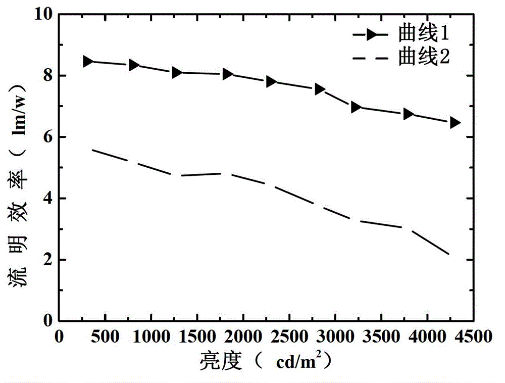
[0055] The structure of the organic electroluminescence device of the present embodiment is: ITO / WO 3 / NPB / Alq 3 / TAZ / Bphen / TAZ:Li 2 CO 3 / MoO3 :F4-TCNQ / TAPC / Alq 3 / TPBi / Cs 2 CO 3 / Ag.

[0056] The preparation of the organic electroluminescent device of this embodiment is as follows:

[0057] (1) Provide the ITO anode substrate. First, the ITO anode substrate is photolithographically processed and cut into the required size, and then the cut ITO anode substrate is sequentially placed in detergent, deionized water, propanol, ethanol and isopropyl ketone Ultrasonic cleaning for 15 minutes in order to remove organic pollutants on the ITO anode substrate.

[0058] (2) The hole injection layer, the first hole transport layer, the first light-emitting layer and the first electron transport layer are formed by vacuum evaporation sequentially on the ITO anode substrate: the material of the hole injection layer is tungsten trioxide (WO 3 ), the thickness is 40 nanometers; the m...

Embodiment 2

[0064] The structure of the organic electroluminescence device of the present embodiment is: AZO / V 2 o 5 / TCTA / BC Z VBi / TAZ / TPBi / Bphen:LiF / V 2 o 5 :2T-NATA / NPB / BC Z VBi / TPBi / CsN 3 / Pt.

[0065] The preparation of the organic electroluminescent device of this embodiment is as follows:

[0066] (1) Provide the AZO anode substrate. First, the AZO anode substrate is photolithographically processed and cut into the required size, and then the cut AZO anode substrate is sequentially placed in detergent, deionized water, propanol, ethanol and isopropyl ketone Ultrasonic cleaning for 15 minutes in order to remove the organic pollutants on the AZO anode substrate.

[0067] (2) On the AZO anode substrate, the hole injection layer, the first hole transport layer, the first light emitting layer and the first electron transport layer are formed by vacuum evaporation in sequence: the material of the hole injection layer is vanadium pentoxide (V 2 o 5 ), the thickness is 80 nanomete...


PUM


Abstract

An organic light emitting device comprises an anode substrate, a hole injection layer, a first hole transport layer, a first light emitting layer, a first electron transport layer, a charge generation layer, a second hole transport layer, a second light emitting layer, a second electron transport layer, an electron injection layer and a cathode layer which are sequentially stacked. The charge generation layer comprises a transport layer, an n-type doped layer and a P-type doped layer which are sequentially stacked. The transport layer is stacked on the first electron transport layer, and is made of a first electron transport material. Materials of the n-type doped layer include a second electron transport material and cesium salt doped in the second electron transport material, and the mass ratio of cesium salt to the second electron transport material is 0.1-0.4:1. Materials of the p-type doped layer include a hole injection material and a p-type doping agent doped in the hole injection material. The organic light emitting device has high luminous efficiency. In addition, the invention relates to a preparation method of the organic light emitting device.

Description

technical field [0001] The invention relates to the field of electronic devices, in particular to an organic electroluminescent device and a preparation method thereof. Background technique [0002] In 1987, C.W.Tang and Van Slyke of Eastman Kodak Company in the United States reported a breakthrough in the research of organic electroluminescence. A high-brightness, high-efficiency double-layer organic electroluminescent device (OLED) has been prepared using ultra-thin film technology. In this double-layer structure device, the brightness reaches 1000cd / m at 10V 2 , its luminous efficiency is 1.51lm / W, and its lifespan is more than 100 hours. [0003] The principle of OLED light emission is based on the action of an external electric field, electrons are injected from the cathode to the lowest unoccupied molecular orbital (LUMO) of organic matter, and holes are injected from the anode to the highest occupied orbital (HOMO) of organic matter. Electrons and holes meet, recom...

Claims


Application Information

Patent Timeline
Patent Type & Authority Applications(China)
IPC IPC(8): H01L51/50H01L51/56
CPCH10K71/166H10K85/631H10K85/324H10K50/165H10K50/17
Inventor 周明杰王平黄辉张振华
Owner OCEANS KING LIGHTING SCI&TECH CO LTD
Why Eureka
Try Eureka