Preparation method and application of 1550 nm long wavelength vertical-cavity surface-emitting laser

A vertical cavity surface emission and laser technology, applied in lasers, laser parts, semiconductor lasers, etc., can solve the problems of hindering the development of long-wavelength VCSEL devices, difficult to realize and prepare current confinement layers, high reflectivity, etc., and achieve compact structure. , the demodulation speed is fast, the cost is low

Inactive Publication Date: 2014-09-17
TIANJIN POLYTECHNIC UNIV
View PDF4 Cites 19 Cited by
  • Summary
  • Abstract
  • Description
  • Claims
  • Application Information

AI Technical Summary

Problems solved by technology

It is difficult to form a high-reflectivity, low-resistance DBR mirror that matches the long-wavelength active gain region; the thermal problem of long-wavelength VCSEL devices is also more significant, and the quaternary or ternary semiconductor materials used in long-wavelength VCSELs are more complex tha

Method used


Image

  • Preparation method and application of 1550 nm long wavelength vertical-cavity surface-emitting laser
  • Preparation method and application of 1550 nm long wavelength vertical-cavity surface-emitting laser
  • Preparation method and application of 1550 nm long wavelength vertical-cavity surface-emitting laser

Examples


Example Embodiment

[0023] Example 1:

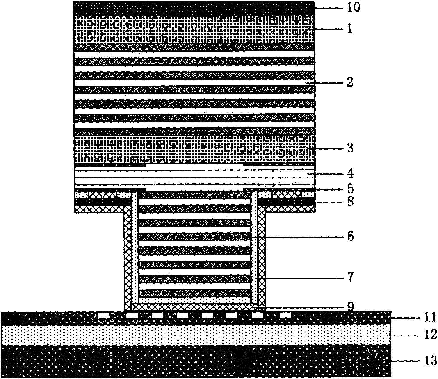
[0024] In the first step, the substrate (1), the N-type DBR (2), the extended InP layer (3), the active area and the epitaxial wafer of the P-type DBR (6) are prepared by the epitaxial growth method;

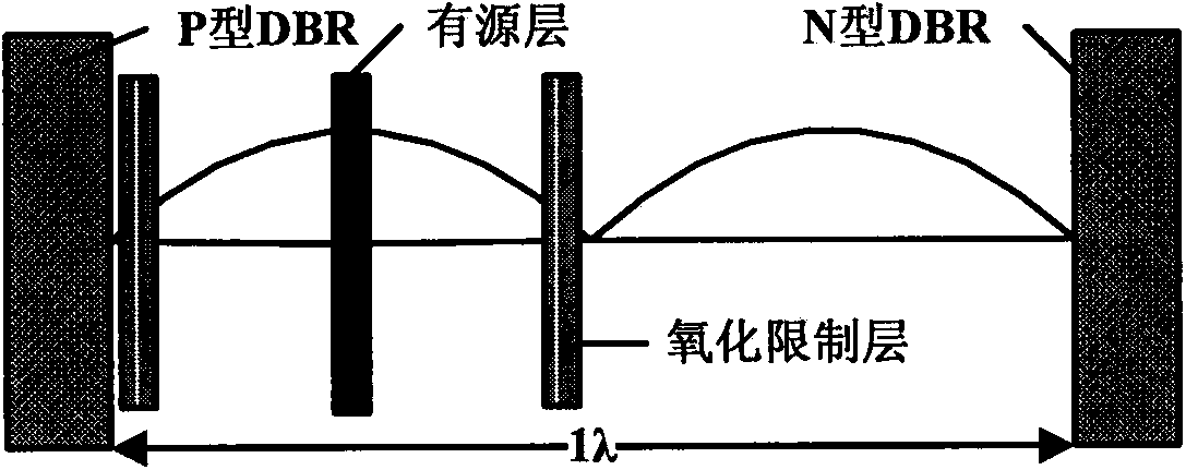
[0025] Prepare the InP substrate (1) and the extended InP layer (3), the thicknesses of which are about 500nm and 775nm, respectively; then use the epitaxial growth method to grow N-type alternately composed of 35 pairs of AlGaAsSb / AlAsSb materials with gradual composition DBR(2), which requires the use of photoresist as a mask for wet chemical etching of N-type DBR. From the formula L=λ / 4n, the thickness of AlGaAsSb and AlAsSb is set to 110nm and 125nm respectively; The graded 31 pairs of AlGaAsSb / AlAsSb alternately composed of N-type DBR (6) have the same material and thickness as the N-type DBR (2); the active area is composed of 3 pairs of InGaAsN / AlGaInAs QWs and two oxidation confinement layers, The cavity length of the resonant cavity is 1λ;

[0026] In the...

Example Embodiment

[0033] Example 2:

[0034] A 1550nm long-wavelength vertical cavity surface emitting laser with InGaAsN / AlGaInAs quantum wells as the active layer, including sequentially connected InP substrate layers, N-type DBR, InP expansion layers, quantum well active gain layers QWs, oxidation confinement layers, P-type DBR (6), insulating layer SiO 2 And N-type and P-type metal electrodes. The multi-quantum well active gain layer QWs of the vertical cavity surface emitting laser resonator cavity is composed of InGaAsN / AlGaInAs material. Using the epitaxial growth method, P-type DBR and N-type DBR are grown by 31 pairs and 35 pairs of AlGaAsSb / AlAsSb materials with gradual composition. In this implementation case, photoresist is required as a mask, and wet chemical etching is performed on both the P-type DBR and the active area. Spin-coating photoresist on the top of the P-type DBR, and perform wet chemical etching on the P-type DBR and the active area to form a cylindrical mesa with the ...

Example Embodiment

[0035] Example 3:

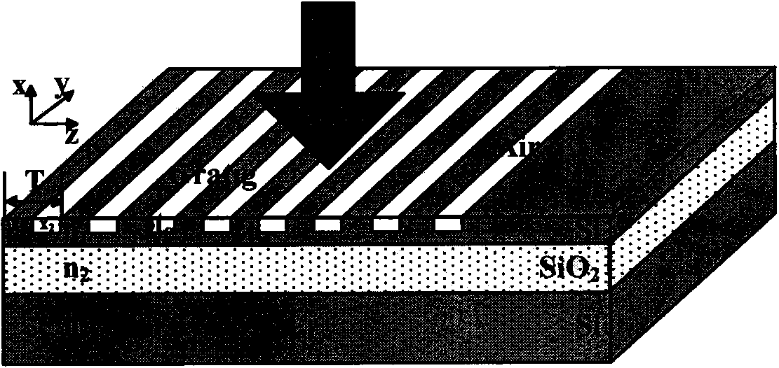
[0036] A 1550nm long-wavelength vertical cavity surface emitting laser with InGaAsN / AlGaInAs quantum wells as the active layer is used for integration with gratings. On the basis of embodiment 1 or 2, continue to be above the P-type mesa and on the left and right sides Re-deposit SiO by using PECVD method 2 . The SiO 2 The insulating layer can prevent the subsequent spin-coated BCB adhesive from damaging the metal electrode, so it has a good protective effect; finally on the device P-type DBR mesa, that is, SiO 2 BCB glue is applied to the top of the protective layer, which can then be connected with the grating part. The BCB layer can reduce the capacitance of the device, thereby not significantly reducing the high-frequency characteristics of the laser.

[0037] It should be noted that the above definition of each element is not limited to the specific structure, shape or size mentioned in the embodiments, and those skilled in the art can easily and well-know...


PUM

PropertyMeasurementUnit
Thicknessaaaaaaaaaa

Abstract

The invention discloses a 1550 nm long wavelength vertical-cavity surface-emitting laser with an InGaAsN/AlGaInAs QWs as an active layer. The laser is characterized in that the InP-based InGaAsN/AlGaInAs QWs and AlGaAsSb/AlAsSb are used as DBR materials of the active layer. The length of a resonant cavity of the laser is 1 lambda so that the better light emitting effect can be achieved. In addition, the performance of the surface-emitting laser is further improved by the adoption of a double-layer oxidation limiting layer structure, single-mode output power is improved, and 1550 nm long wavelength transmission is achieved. The laser comprises a P-type DBR layer, the active layer, an N-type DBR layer, a substrate, a SiO2 insulating layer, a transparent conducting medium ZnO, a P-type electrode and an N-type back electrode. The whole structure achieves lattice matching in material, so that the epitaxy technology can be widely applied. The vertical-cavity surface-emitting laser is simple in manufacturing technology, good in repeatability and easy to popularize.

Description

Technical field [0001] The invention relates to a method for manufacturing a vertical cavity surface emitting laser with a long-wavelength InGaAsN / AlGaInAs quantum well as an active layer and its coupling with a grating. It has important applications in optoelectronic integration and belongs to the field of semiconductor lasers. Background technique [0002] In the semiconductor optoelectronics industry, semiconductor lasers can emit lasers only with a very low current supply, and because of their small size, they solve the insurmountable difficulties caused by the scaling down of feature sizes in optoelectronic integration, and are called micro lasers. Relying on its advantages of easy integration with other devices and long working life, this low-cost, high-performance light source has become more and more prominent in the system and is receiving more and more attention. Semiconductor lasers can be divided into two types according to the angle of laser emission: Edge-Emitting L...

Claims


Application Information

Patent Timeline
IPC IPC(8): H01S5/183
Inventor 李鸿强崔贝贝周文骞刘宇
Owner TIANJIN POLYTECHNIC UNIV
Why Eureka
Try Eureka