Zinc oxide film imaging method

A zinc oxide thin film and patterning technology, applied in ion implantation plating, metal material coating process, coating, etc., can solve the problems of poor etching pattern accuracy, cumbersome operation, and difficult control of etching time, etc., and achieve good Good electrical conductivity and light transmission, excellent dielectric properties, and good application prospects

Inactive Publication Date: 2014-10-08
TIANJIN UNIV
View PDF2 Cites 6 Cited by
  • Summary
  • Abstract
  • Description
  • Claims
  • Application Information

AI Technical Summary

Problems solved by technology

Dry etching equipment is expensive and the process is complicated, and the operation is cumbersome. The wet etching process is simple and easy to operate, but the etching rate is particularly sensitive to influencing factors, the etching time is not easy to control, and the accuracy of the etching pattern is poor.

Method used


Image

  • Zinc oxide film imaging method

Examples


Embodiment 1

[0027] (1) Cleaning substrate and photolithography development

[0028] (a) putting the silicon substrate into an acetone organic solvent for ultrasonic cleaning, rinsing with deionized water and drying in a nitrogen stream;

[0029] (b) The photoresist is spin-coated on the silicon substrate, the coating thickness is 1um, and the photolithography mask is used for exposure processing;

[0030] (c) using a developer to develop the electrode pattern;

[0031] (2) Put the developed silicon substrate into the vacuum chamber of the magnetron sputtering apparatus, install the zinc oxide target material on the corresponding radio frequency target, and use the radio frequency magnetron sputtering method to deposit the zinc oxide film;

[0032] (3) After the step (2) is finished, take out the silicon substrate, peel off the substrate in an acetone organic solvent, and obtain the desired zinc oxide film pattern after peeling off.

Embodiment 2~5

[0034] The process steps of Examples 2-5 are the same as those of Example 1, except that the coating thickness and film thickness of the photoresist spin-coated on the substrate are different from the substrate and organic solvent used.

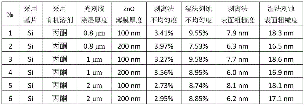
[0035] The main process parameters of the present invention and the non-uniformity comparison of the ZnO film obtained by the stripping method and the wet etching method in the present invention are shown in Table 1. By comparison, it can be seen that under the same conditions, the pattern accuracy of the film obtained by the lift-off method is higher than that obtained by wet etching (the unevenness of the film obtained by the lift-off method is smaller than that of the film obtained by wet etching ), and the surface roughness of the film obtained by the peeling method is smaller.

[0036] Table 1

[0037]

[0038] Inhomogeneity in Table 1 = (d max -d min ) / (d max +d min ); d max is the maximum film thickness, d min is the minimum ...


PUM

PropertyMeasurementUnit
thicknessaaaaaaaaaa

Abstract

The invention discloses a zinc oxide film imaging method comprising the following steps of firstly, cleaning a substrate, photoetching and developing to obtain an imaged photoresist; secondly, placing the substrate into a vacuum chamber to deposit a ZnO film with the thickness of 100-200nm; finally, ultrasonically stripping the substrate in an organic solvent to obtain an imaged zinc oxide film. The zinc oxide film imaging method is simple in process; the imaged zinc oxide film is high in image precision, favorable in dielectric property and good in application prospect and has favorable conductivity and light transparency.

Description

technical field [0001] The invention belongs to the field of electronic information materials and components, in particular to a new patterning method for fully transparent thin film transistor materials. Background technique [0002] Transparent conductive films are widely used in a variety of optoelectronic devices, such as solar transparent electrodes, energy-saving windows, and flat-panel liquid crystal displays, due to their excellent optoelectronic properties such as transparency in visible light and low resistivity. Currently the most widely used is the ITO transparent conductive film, because ITO contains expensive and scarce metal indium, resulting in high cost. Compared with ITO, ZnO thin film has a wider forbidden band width and high transmittance in the visible light range, and the resistivity can be reduced by doping with Al, Ga, In, etc. Moreover, the ZnO transparent conductive thin film has rich raw materials, low cost, good chemical stability, easy large-sca...

Claims


Application Information

Patent Timeline
Patent Type & Authority Applications(China)
IPC IPC(8): C23C14/04C23C14/35C23C14/08
Inventor 李玲霞许丹于士辉董和磊金雨馨
Owner TIANJIN UNIV
Why Eureka
Try Eureka