Double-nested copper interconnection structure and fabrication method thereof

A technology of copper interconnection structure and manufacturing method, which is applied in semiconductor/solid-state device manufacturing, electrical components, electric solid-state devices, etc., can solve the problems of device open-circuit contact resistance, diffusion barrier copper easily diffused into the medium, and device short-circuit, etc. Achieve the effects of avoiding short circuit of the device, improving reliability and anti-electromigration ability, and enhancing adhesion

Active Publication Date: 2014-10-22
SEMICON MFG INT (SHANGHAI) CORP
View PDF5 Cites 12 Cited by
  • Summary
  • Abstract
  • Description
  • Claims
  • Application Information

AI Technical Summary

Problems solved by technology

[0006] In view of the above-mentioned shortcomings of the prior art, the object of the present invention is to provide a dual-nested copper interconnection structure and a manufacturing method thereof, which are used to solve the problems caused by the poor adhesion between the metal and the medium in the prior art. The phenomenon of open circuit or high contact resistance, and the problem that the diffusion barrier layer is too thin makes copper easy to diffuse into the medium and cause short circuit of the device

Method used


Image

  • Double-nested copper interconnection structure and fabrication method thereof
  • Double-nested copper interconnection structure and fabrication method thereof
  • Double-nested copper interconnection structure and fabrication method thereof

Examples


Embodiment 1

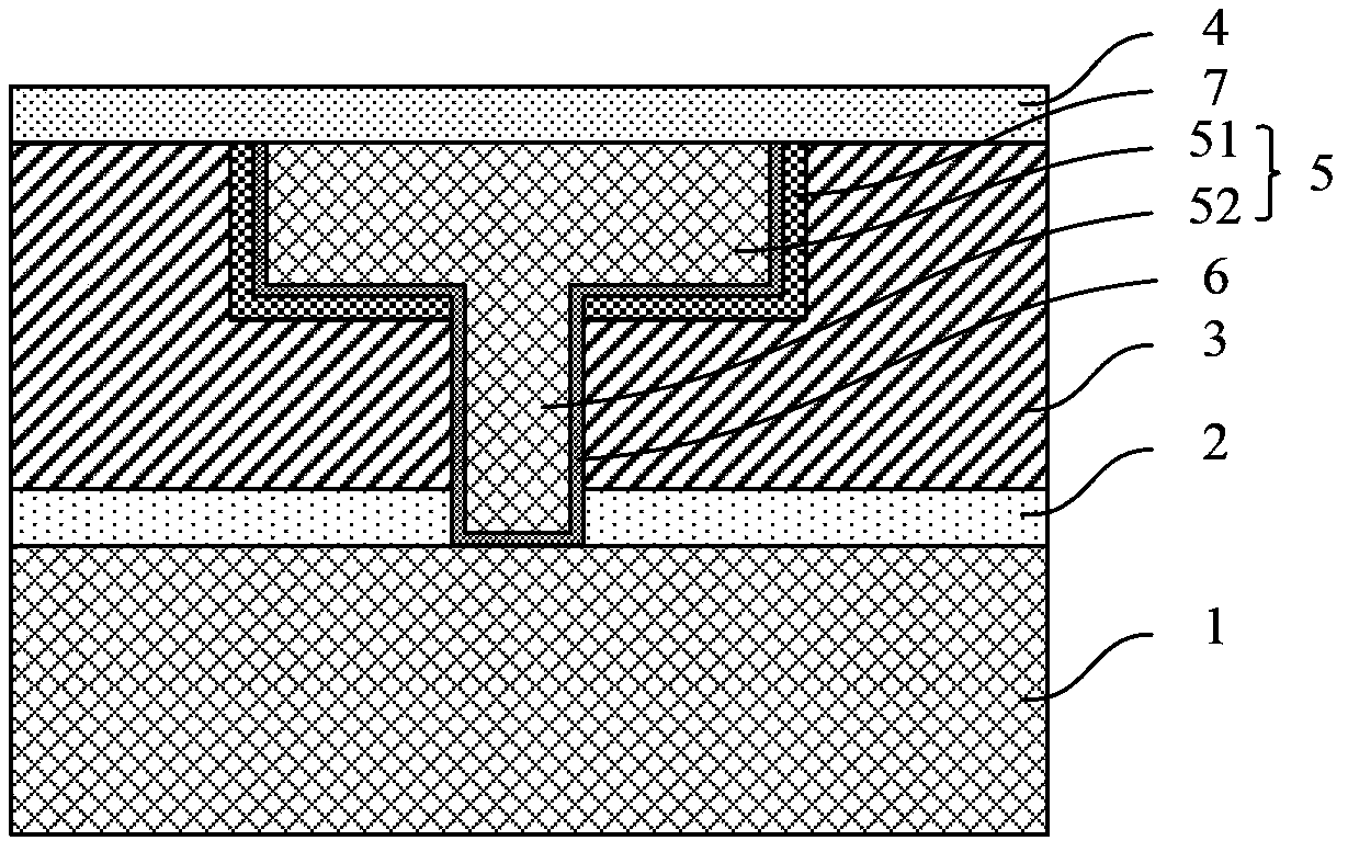
[0057] The present invention provides a dual-nested copper interconnect structure, see figure 1, which is a schematic cross-sectional structure diagram of the dual nested copper interconnection structure of the present invention. As shown in the figure, the dual nested copper interconnection structure at least includes: a first copper layer 1, which is sequentially formed on the first copper layer The first cap layer 2, the interlayer dielectric layer 3 and the second cap layer 4; the second copper layer 5 for conductive interconnection is formed in the interlayer dielectric layer 3 and the first cap layer 2, and the The upper surface of the second copper layer 5 is connected to the lower surface of the second cap layer 4, and the remaining part of the second copper layer 5 except the upper surface is surrounded by a metal diffusion barrier layer 6, and the metal diffusion barrier layer 6, the bottom is connected to the upper surface of the first copper layer 1; the second cop...

Embodiment 2

[0077] Embodiment 2 adopts basically the same technical solution as Embodiment 1, except that the structure of the nitrogen-doped layer in the double-nested copper interconnection structure is different. In the double-nested copper interconnection structure of the first embodiment, only the nitrogen-doped layer is around the metal wiring, while in the double-nested copper interconnection structure of the second embodiment, there are nitrogen-doped layers around the metal wiring and the conductive plug, further Improve the adhesion between metal and medium and metal diffusion barrier ability.

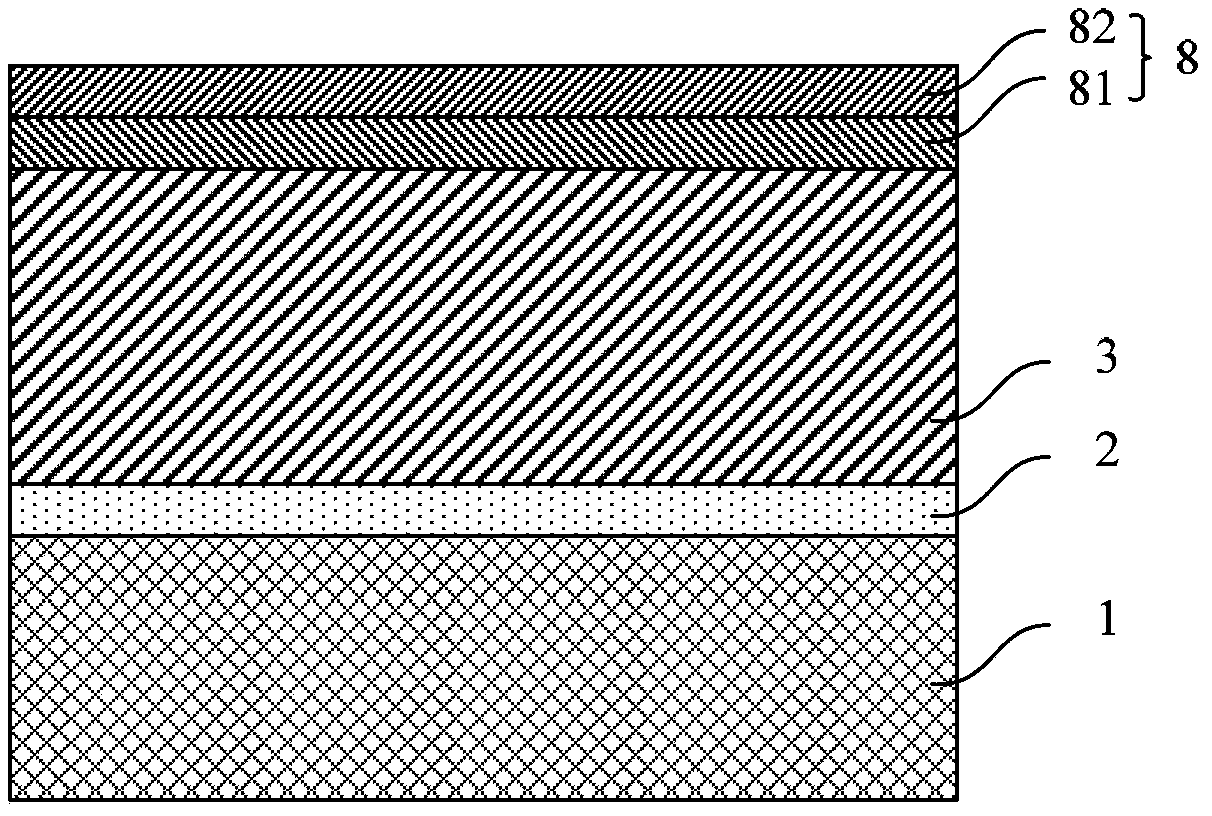
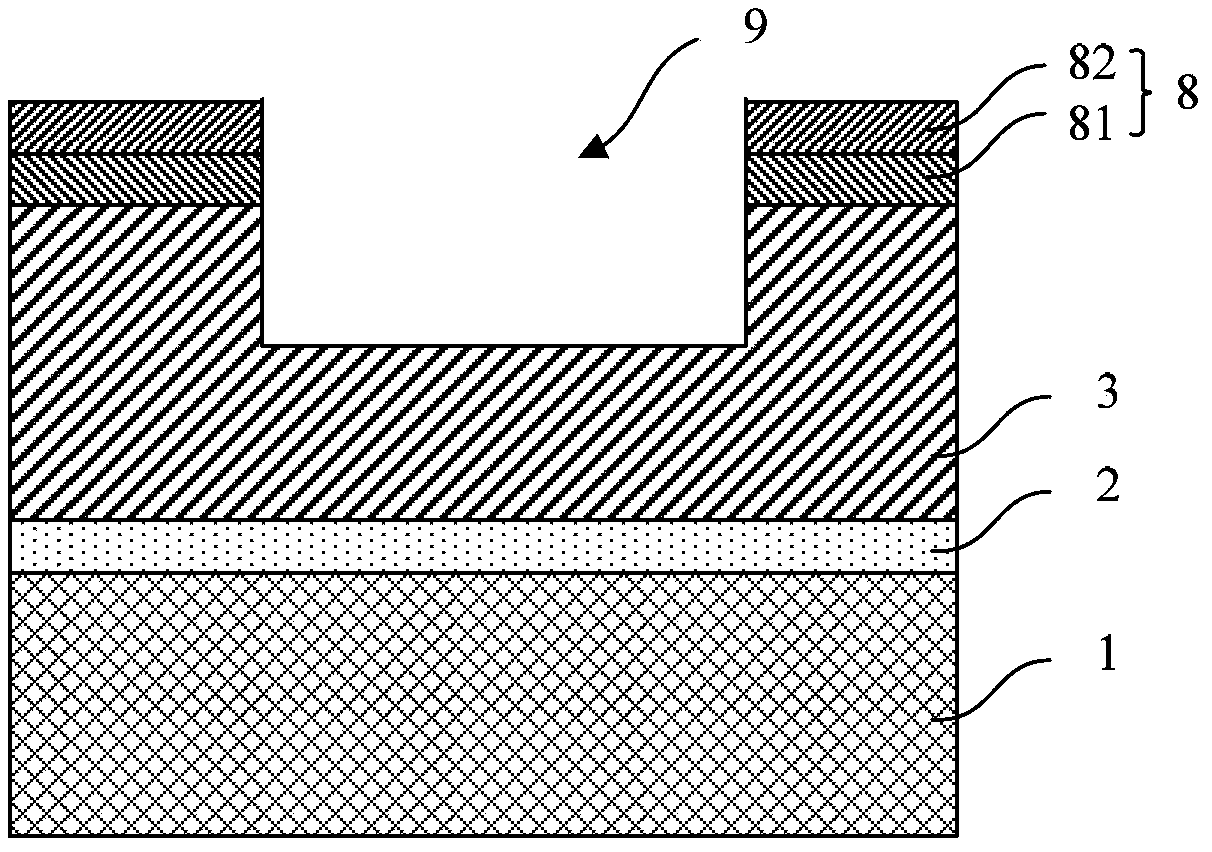
[0078] The present invention provides a dual-nested copper interconnect structure, see Figure 10 , which is a schematic cross-sectional structure diagram of the dual nested copper interconnection structure of the present invention. As shown in the figure, the dual nested copper interconnection structure at least includes: a first copper layer 1, which is sequentially formed on the first...


PUM

PropertyMeasurementUnit
thicknessaaaaaaaaaa

Abstract

The invention provides a double-nested copper interconnection structure and a fabrication method thereof. In the double-nested copper interconnection structure, the metal diffusion barrier layer on the surface of a metal connection line is surrounded by a nitrogen-doped layer, or the metal diffusion barrier layer of the partial surface of the metal connection line and a conductive plug that located in an interlayer dielectric layer is surrounded by a nitrogen-doped layer. The nitrogen-doped layer is obtained through nitrogen or ammonia gas plasma treatment. The nitrogen-doped layer can be used to improve the adhesive power between the interlayer dielectric layer and metal, and the mechanical strength between the nitrogen-doped layer and a second cap layer is higher, so that the adhesive power between copper and the second cap layer can be further improved, the electromigration resistance of devices can be improved, and the nitrogen-doped layer can also be used to further prevent copper from being diffused into the interlayer dielectric on the basis of the metal diffusion barrier layer to prevent the short-circuit phenomenon from occurring on the devices.

Description

technical field [0001] The invention belongs to the field of semiconductor manufacturing, and relates to an interconnection structure and a manufacturing method thereof, in particular to a double-nested copper interconnection structure and a manufacturing method thereof. Background technique [0002] With the rapid development of integrated circuit CMOS technology in accordance with Moore's Law, interconnection delay gradually replaces device delay as a key factor affecting chip performance. The parasitic capacitance and interconnection resistance between the interconnections cause the transmission delay of the signal. Since copper has low resistivity, excellent anti-electromigration characteristics and high reliability, it can reduce the interconnection resistance of the metal, thereby reducing the overall interconnection delay effect, and has now changed from conventional aluminum interconnection to low Resistor copper interconnects. At the same time, reducing the capaci...

Claims


Application Information

Patent Timeline
Patent Type & Authority Applications(China)
IPC IPC(8): H01L23/522H01L21/768
Inventor 肖德元徐依协
Owner SEMICON MFG INT (SHANGHAI) CORP
Why Eureka
Try Eureka