Organic light-emitting device and preparation method thereof

An electroluminescent device and luminescent technology, which is applied in the direction of electric solid-state devices, semiconductor/solid-state device manufacturing, electrical components, etc., can solve the problems of poor refractive index, total reflection loss, low light extraction performance, etc., and achieve stable film layer, Reduce the injection barrier and improve the effect of outgoing light

Inactive Publication Date: 2014-10-29
OCEANS KING LIGHTING SCI&TECH CO LTD +2
View PDF5 Cites 6 Cited by
  • Summary
  • Abstract
  • Description
  • Claims
  • Application Information

AI Technical Summary

Problems solved by technology

[0004] In traditional light-emitting devices, only about 18% of the light inside the device can be emitted to the outside, while the rest will be consumed outside the device in other forms, and there is a difference in refractive index between the interfaces (such as between gla

Method used


Image

  • Organic light-emitting device and preparation method thereof
  • Organic light-emitting device and preparation method thereof

Examples


Embodiment 1

[0045] A method for preparing an organic electroluminescent device, comprising the following steps:

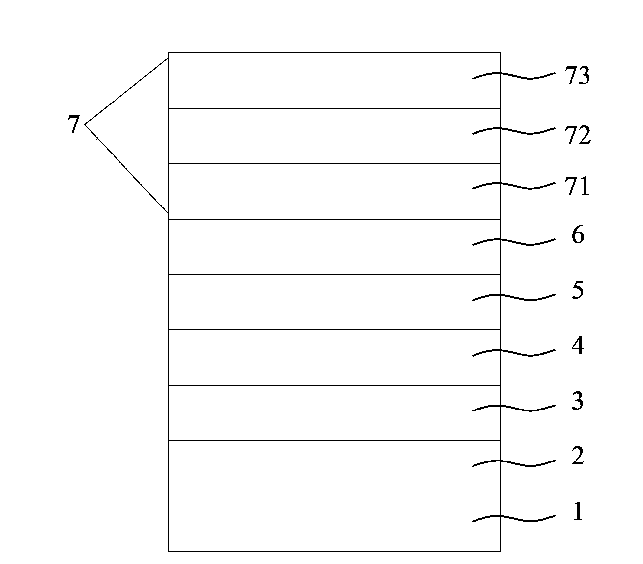
[0046] (1) First, the ITO glass substrate is subjected to photolithography treatment, and then cut into 2×2cm 2 Then use detergent, deionized water, acetone, ethanol, and isopropanol to ultrasonicate for 15 minutes each to remove organic pollutants on the glass surface, clean them and air dry them; then use thermal resistance evaporation on the anode Prepare hole injection layer, hole transport layer, light-emitting layer, electron transport layer and electron injection layer in sequence; Wherein,

[0047] The hole injection layer is made of MoO 3 , the pressure used in evaporation is 8×10 -5 Pa, the evaporation rate is 3nm / s, and the evaporation thickness is 25nm;

[0048] The material of the hole transport layer is NPB, and the pressure used during evaporation is 8×10 -5 Pa, the evaporation rate is 0.2nm / s, and the evaporation thickness is 45nm;

[0049] The material of...

Embodiment 2

[0059] A method for preparing an organic electroluminescent device, comprising the following steps:

[0060] (1) First, the AZO glass substrate is subjected to photolithography treatment, and then cut into 2×2cm 2 Then use detergent, deionized water, acetone, ethanol, and isopropanol to ultrasonicate for 15 minutes each to remove organic pollutants on the glass surface, clean them and air dry them; then use thermal resistance evaporation on the anode Prepare hole injection layer, hole transport layer, light-emitting layer, electron transport layer and electron injection layer in sequence; Wherein,

[0061] The material of the hole injection layer is WO 3 , the pressure used in evaporation is 2×10 -3 Pa, the evaporation rate is 10nm / s, and the evaporation thickness is 80nm;

[0062] The material of the hole transport layer is TCTA, and the pressure used during evaporation is 2×10 -3 Pa, the evaporation rate is 0.1nm / s, and the evaporation thickness is 60nm;

[0063] The ma...

Embodiment 3

[0073] A method for preparing an organic electroluminescent device, comprising the following steps:

[0074] (1) First, the IZO glass substrate is subjected to photolithography treatment, and then cut into 2×2cm 2 Then use detergent, deionized water, acetone, ethanol, and isopropanol to ultrasonicate for 15 minutes each to remove organic pollutants on the glass surface, clean them and air dry them; then use thermal resistance evaporation on the anode Prepare hole injection layer, hole transport layer, light-emitting layer, electron transport layer and electron injection layer in sequence; Wherein,

[0075] The material of the hole injection layer is V 2 o 5 , the pressure used in evaporation is 5×10 -5 Pa, the evaporation rate is 1nm / s, and the evaporation thickness is 20nm;

[0076] The material of the hole transport layer is TAPC, and the pressure used during evaporation is 5×10 -5 Pa, the evaporation rate is 1nm / s, and the evaporation thickness is 20nm;

[0077] The m...


PUM

PropertyMeasurementUnit
Work functionaaaaaaaaaa
Thicknessaaaaaaaaaa
Thicknessaaaaaaaaaa

Abstract

The invention discloses an organic light-emitting device and a preparation method thereof. The organic light-emitting device consists of a conductive anode glass substrate, a hole injection layer, a hole transport layer, a luminescent layer, an electron transport layer, an electron injection layer and a composite cathode, wherein the layers are successively laminated. The composite anode includes a low-work function metal layer, a metallic oxide doping layer, and a conductive thin film layer, wherein the layers are successively laminated and the work functions of the layers are from 2.0eV to 3.5eV. The energy level difference between lowest unoccupied molecular orbital units of the low-work function metal work function and an organic layer is small, so that the electron injection capability can be effectively improved. The metallic oxide doping layer uses the metallic oxide and the silicon compound to carry out doping; the metallic oxide has high stability and the light transmittance in the visible light range is high; and the silicon compound forms a well-ordered microsphere structure after preparation, thereby carrying out scattering on the light. The conductive thin-film material can reflect the transmitted light and thus the light can be reflected to the bottom of the device; and with the composite electrode, the luminous efficiency can be effectively improved.

Description

technical field [0001] The invention relates to the field of organic electroluminescence, in particular to an organic electroluminescence device and a preparation method thereof. Background technique [0002] In 1987, C.W.Tang and Van Slyke of Eastman Kodak Company in the United States reported a breakthrough in the research of organic electroluminescence. A high-brightness, high-efficiency double-layer organic electroluminescent device (OLED) has been prepared using ultra-thin film technology. Brightness up to 1000cd / m at 10V 2 , its luminous efficiency is 1.51lm / W, and its lifespan is more than 100 hours. [0003] The principle of OLED light emission is based on the action of an external electric field, electrons are injected from the cathode to the lowest unoccupied molecular orbital (LUMO) of organic matter, and holes are injected from the anode to the highest occupied orbital (HOMO) of organic matter. Electrons and holes meet, recombine, and form excitons in the ligh...

Claims


Application Information

Patent Timeline
IPC IPC(8): H01L51/52H01L51/54H01L51/56
CPCH10K50/826H10K50/854H10K50/856
Inventor 周明杰黄辉张振华王平
Owner OCEANS KING LIGHTING SCI&TECH CO LTD
Why Eureka
Try Eureka