Epitaxial wafer, growing method and LED structure of Mg-doped electronic barrier layer

An electron blocking layer and growth method technology, applied in circuits, electrical components, semiconductor devices, etc., can solve problems such as restricting the brightness improvement of gallium nitride-based LEDs, and achieve the effects of improving light extraction efficiency, increasing brightness, and increasing the amount of holes

Active Publication Date: 2014-11-05
XIANGNENG HUALEI OPTOELECTRONICS
View PDF7 Cites 30 Cited by
  • Summary
  • Abstract
  • Description
  • Claims
  • Application Information

AI Technical Summary

Problems solved by technology

[0004] The purpose of the present invention is to overcome the above disadvantages and provide an epitaxial wafer with a Mg-doped el...

Method used


Image

  • Epitaxial wafer, growing method and LED structure of Mg-doped electronic barrier layer
  • Epitaxial wafer, growing method and LED structure of Mg-doped electronic barrier layer

Examples


Embodiment 1

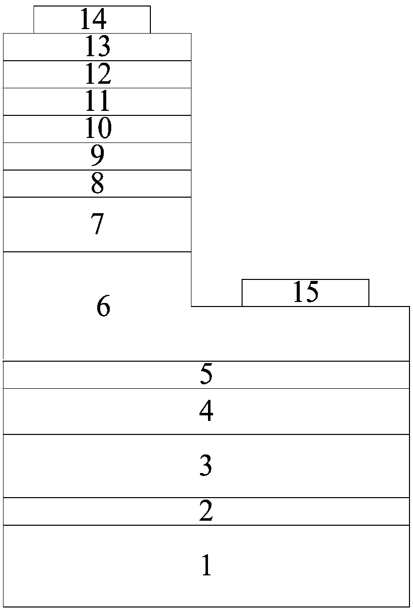
[0037] Please refer to figure 1 , the Mg-doped electron blocking layer LED epitaxial wafer of the present invention is sequentially from bottom to top: substrate 1, low-temperature GaN buffer layer 2, high-temperature GaN buffer layer 3, n-type GaN layer 4, n-type AlGaN layer 5, n-type A contact layer 6, a multi-quantum well layer 7, a GaN barrier layer 8, an AlGaN / GaN electron blocking layer 9 on the GaN barrier layer 8, and a low-temperature P-type GaN layer on the AlGaN / GaN electron blocking layer 9 10. On the low-temperature P-type GaN layer 10 is a high-concentration AlGaN / InGaN electron blocking layer 11 doped with Mg, and on the above-mentioned AlGaN / InGaN electron blocking layer 11 is a high-temperature P-type GaN layer 12, and the On the high-temperature P-type GaN layer 12 is a P-type contact layer 13, and a P-electrode 14 and an N-electrode 15 arranged on the epitaxial wafer.

[0038] The method for growing the epitaxial wafer of the Mg-doped electron blocking laye...

Embodiment 2

[0048] In the method of this embodiment: the steps of processing the substrate, the low-temperature GaN buffer layer, the high-temperature GaN buffer layer, the n-type GaN layer, the n-type AlGaN layer, the n-type contact layer, the multi-quantum well layer, and the GaN barrier layer are the same as in Embodiment 1. ,Also includes:

[0049] An AlGaN / GaN electron blocking layer is grown on the GaN barrier layer, the blocking layer is an unintentionally doped AlGaN / GaN superlattice structure, the growth temperature is 810°C, and the Al concentration is 1E+20atom / cm 3 , total thickness 8nm.

[0050] A low-temperature P-type GaN layer is grown on the AlGaN / GaN electron blocking layer, the growth temperature is 700°C, and the thickness is 50nm.

[0051] A high-concentration AlGaN / InGaN electron blocking layer doped with Mg is grown on the low-temperature P-type GaN layer, the growth temperature is 900°C, and the Al concentration is 1E+20 atom / cm 3 , Mg concentration in 1E+20~1E+2...

Embodiment 3

[0055] In the method of this embodiment: the steps of processing the substrate, the low-temperature GaN buffer layer, the high-temperature GaN buffer layer, the n-type GaN layer, the n-type AlGaN layer, the n-type contact layer, the multi-quantum well layer, and the GaN barrier layer are the same as in Embodiment 1. ,Also includes:

[0056] An AlGaN / GaN electron blocking layer is grown on the GaN barrier layer, the blocking layer is an unintentionally doped AlGaN / GaN superlattice structure, the growth temperature is 850°C, and the Al concentration is 1E+20atom / cm 3 , total thickness 12nm.

[0057] A low-temperature P-type GaN layer is grown on the AlGaN / GaN electron blocking layer, the growth temperature is 800°C, and the thickness is 80nm.

[0058] A high-concentration AlGaN / InGaN electron blocking layer doped with Mg is grown on the low-temperature P-type GaN layer, the growth temperature is 1000°C, and the Al concentration is 1E+20 atom / cm 3 , Mg concentration in 1E+20~1E...


PUM

PropertyMeasurementUnit
Thicknessaaaaaaaaaa
Thicknessaaaaaaaaaa
Total thicknessaaaaaaaaaa

Abstract

The invention discloses an epitaxial wafer, growing method and LED structure of an Mg-doped electronic barrier layer. The epitaxial wafer comprises a substrate, a low-temperature GaN buffer layer, a high-temperature GaN buffer layer, an n type GaN layer, an n type AlGaN layer, an n type contact layer, a multiple quantum well layer and a GaN base layer from bottom to top in sequence. An AlGaN/GaN electronic barrier layer is arranged on the GaN base layer, a low-temperature P type GaN layer is arranged on the AlGaN/GaN electronic barrier layer, a high-concentration AlGaN/InGaN electronic barrier layer doped with Mg is arranged on the low-temperature P type GaN layer, a high-temperature P type GaN layer is arranged on the AlGaN/InGaN electronic barrier layer, and a P type contact layer is arranged on the high-temperature P type GaN layer. The epitaxial wafer, growing method and LED structure of the Mg-doped electronic barrier layer have the advantages that the hole concentration of the part injected into multiple quantum wells of a P layer is improved, and the barrier function of electrons is improved so that the luminous efficiency can be improved, and the brightness can be obviously improved.

Description

technical field [0001] The invention belongs to the technical field of semiconductors, and relates to an epitaxial wafer of a Mg-doped electron blocking layer, a growth method and an LED structure. Background technique [0002] Gallium nitride-based materials, including InGaN, GaN, and AlGaN alloys, are direct bandgap semiconductors, and the bandgap is continuously adjustable from 1.8-6.2eV. They have excellent properties such as wide direct bandgap, strong chemical bonds, high temperature resistance, and corrosion resistance. It is an ideal material for the production of short-wavelength high-brightness light-emitting devices, ultraviolet light detectors and high-temperature and high-frequency microelectronic devices. It is widely used in full-color large-screen displays, LCD backlights, signal lights, lighting and other fields. There are two ways to improve the luminous efficiency of GaN-based LEDs: 1. Improve the internal quantum efficiency; 2. Improve the external quantu...

Claims


Application Information

Patent Timeline
IPC IPC(8): H01L33/14H01L33/06H01L33/00
CPCH01L33/0075H01L33/06H01L33/145
Inventor 周少将徐迪卢国军刘为刚
Owner XIANGNENG HUALEI OPTOELECTRONICS
Why Eureka
Try Eureka