Organic light emitting device (OLED) and manufacturing method thereof
An electroluminescent device and a luminescent technology, which are applied in the manufacture of organic semiconductor devices, electric solid devices, semiconductor/solid state devices, etc., can solve the problems of unfavorable practical application of OLEDs, poor thermal stability, and reduced service life, and achieve Low cost, stable properties, and improved service life
- Summary
- Abstract
- Description
- Claims
- Application Information
AI Technical Summary
Problems solved by technology
Method used
Image
Examples
Embodiment 1
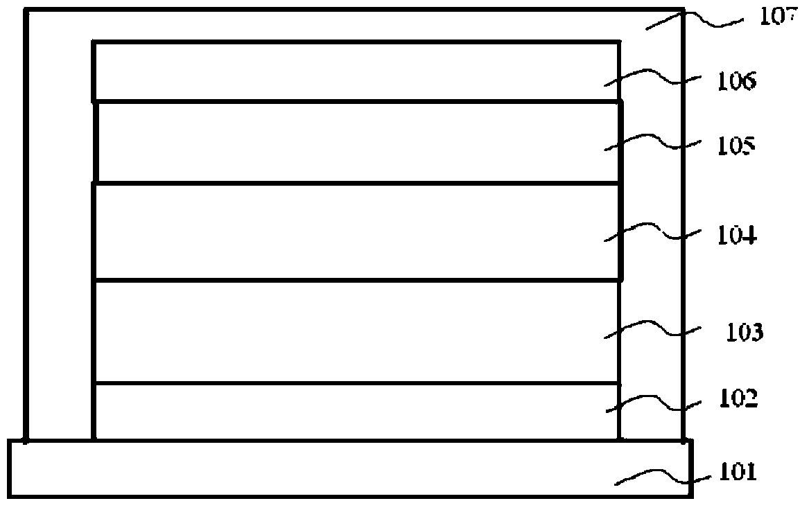
[0062] A method for preparing an organic electroluminescent device, comprising the following steps:
[0063] (1) Put the glass substrate in deionized water containing detergent for ultrasonic cleaning. After cleaning, use isopropanol and acetone in ultrasonic treatment for 20 minutes, and then blow dry with nitrogen to obtain a clean substrate;
[0064] (2) In a vacuum of 1×10 -4 In Pa's vacuum thermal evaporation coating system, Ag is evaporated on the surface of the substrate as the cathode, with a thickness of 18nm and an evaporation speed of 0.5nm / s;
[0065] (3) In a vacuum of 1×10 -4 In Pa's vacuum sputtering coating system, TiO is sputtered on the cathode surface 2 As an electron transport layer, the thickness is 20nm, and the sputtering speed is 0.2nm / s;
[0066] (4) In a vacuum of 1×10 -4 In the vacuum thermal evaporation coating system, the light-emitting layer, the hole transport layer and the anode are sequentially evaporated on the surface of the electron tran...
Embodiment 2
[0073] A method for preparing an organic electroluminescent device, comprising the following steps:
[0074] (1) Put the glass substrate in deionized water containing detergent for ultrasonic cleaning. After cleaning, use isopropanol and acetone in ultrasonic treatment for 20 minutes, and then blow dry with nitrogen to obtain a clean substrate;
[0075] (2) In a vacuum of 1×10 -3 In Pa's vacuum thermal evaporation coating system, Al is evaporated on the surface of the substrate as a cathode with a thickness of 25nm and an evaporation rate of 0.5nm / s;
[0076] (3) In a vacuum of 1×10 -3 In Pa's vacuum sputtering coating system, ZnO is sputtered on the cathode surface as an electron transport layer with a thickness of 10nm and a sputtering speed of 0.2nm / s;
[0077] (4) In a vacuum of 1×10 -3 In the vacuum thermal evaporation coating system, the light-emitting layer, the hole transport layer and the anode are sequentially evaporated on the surface of the electron transport la...
Embodiment 3
[0083] A method for preparing an organic electroluminescent device, comprising the following steps:
[0084] (1) Put the glass substrate in deionized water containing detergent for ultrasonic cleaning. After cleaning, use isopropanol and acetone in ultrasonic treatment for 20 minutes, and then blow dry with nitrogen to obtain a clean substrate;
[0085] (2) In a vacuum of 1×10 -5 In Pa's vacuum thermal evaporation coating system, Sm is evaporated on the surface of the substrate as the cathode, with a thickness of 35nm and an evaporation rate of 0.5nm / s;
[0086] (3) In a vacuum of 1×10 -5 In the vacuum sputtering coating system of Pa, Nb is sputtered on the cathode surface 2 o 5 As an electron transport layer, the thickness is 50nm, and the sputtering speed is 0.2nm / s;
[0087] (4) In a vacuum of 1×10 -5 In the vacuum thermal evaporation coating system, the light-emitting layer, the hole transport layer and the anode are sequentially evaporated on the surface of the elect...
PUM
 Abstract
Description
Claims
Application Information

