Preparation method for zinc tin nitride polycrystalline film
A technology of zinc tin nitride and thin film, which is applied in the direction of ion implantation plating, metal material coating process, coating, etc., can solve the problems of complicated preparation process, high requirements, increased preparation cost, etc., and achieve the reduction of preparation difficulty and reduction The effect of simple production cost and process
- Summary
- Abstract
- Description
- Claims
- Application Information
AI Technical Summary
Problems solved by technology
Method used
Image
Examples
Embodiment 1
[0028] Firstly, the quartz plate substrate is cleaned, and the specific method is: sequentially use acetone, ethanol and deionized water to ultrasonically clean the substrate for 15 minutes each.
[0029] Next, the cleaned quartz wafer substrate and the ZnSn alloy target (the atomic ratio of Zn to Sn is 3:1) are placed in corresponding positions of the magnetron sputtering equipment. The magnetron sputtering equipment is a high-vacuum magnetron sputtering equipment model JZCK-4003 of Shenyang Juzhi Vacuum Equipment Co., Ltd.
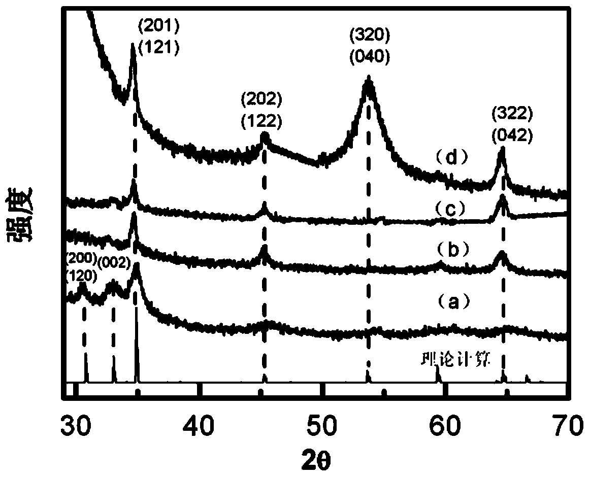
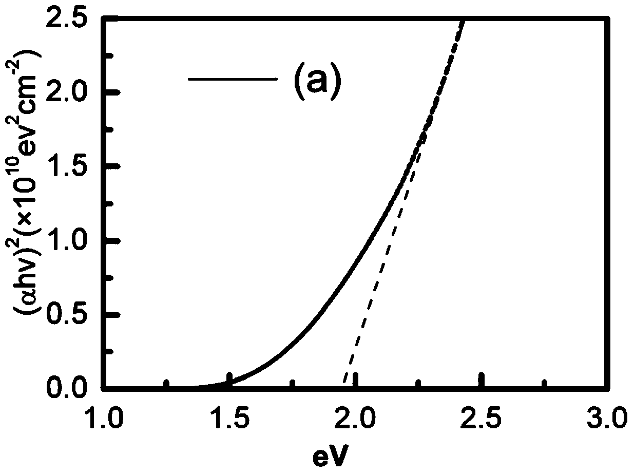
[0030] Sputtering at room temperature, set the background vacuum to 6×10 -4 Pa. The magnetron sputtering method is adopted under vacuum conditions, the sputtering power is 210W, and the working pressure is 1.9Pa. N ions are bombarded on the cathode ZnSn alloy target, so that the target atoms are sputtered and react with N ions to form ZnSnN 2 Deposited on the substrate, forming ZnSnN 2 Polycrystalline film, denoted as sample (a).
Embodiment 2
[0032] The substrate is replaced by a silicon chip substrate, the Zn and Sn atomic ratio of the ZnSn alloy target is 2:1, and other process steps and process parameters are the same as in Example 1, and the prepared ZnSnN 2 The polycrystalline thin film is designated as sample (b).
Embodiment 3
[0034]The substrate is replaced with a glass sheet substrate, the atomic ratio of Zn and Sn of the ZnSn alloy target is 3:1, other process steps and process parameters are the same as those in Example 1, and the prepared ZnSnN 2 The polycrystalline thin film is designated as sample (c).
PUM
 Abstract
Description
Claims
Application Information


