

SiGe (silicon germanium) source and drain area manufacturing method
A manufacturing method and drain region technology, which is applied in semiconductor/solid-state device manufacturing, electrical components, circuits, etc., can solve the problems of increasing the difficulty of SiGe epitaxy process in grooves, the decrease of device yield, and the decrease of process stability, so as to achieve enhanced Effect of process stability, stress increase, avoidance of stress relaxation
- Summary
- Abstract
- Description
- Claims
- Application Information
AI Technical Summary
Problems solved by technology
Method used
Image


Examples
no. 1 example
[0035] see Figure 4 , the manufacturing method of the SiGe source / drain region of the present embodiment comprises the following steps:
[0036] Step S01, providing an N-type wafer silicon substrate formed with gates, and etching grooves for forming source / drain regions on the silicon substrate;
[0037] Step S02, epitaxially growing a SiGe buffer layer in the groove;
[0038] Step S03, epitaxially growing a SiGe main body layer on the buffer layer, the concentration of Ge in the main body layer is higher than that of the buffer layer;
[0039] Step S04, repeating steps S02 to S03 once, that is, growing a buffer layer and a main layer on the main layer grown in step S03 to form a multi-layer structure with alternately stacked buffer layers and main layers;
[0040] Step S05 , epitaxially growing a Si capping layer on the multilayer structure formed in step S04 to form a PMOS source / drain region with SiGe.
[0041]This embodiment adopts the method of alternating SiGe epitax...
no. 2 example
[0043] see Figure 5a to Figure 5h , the manufacturing method of the SiGe source / drain region of the present embodiment comprises the following steps:
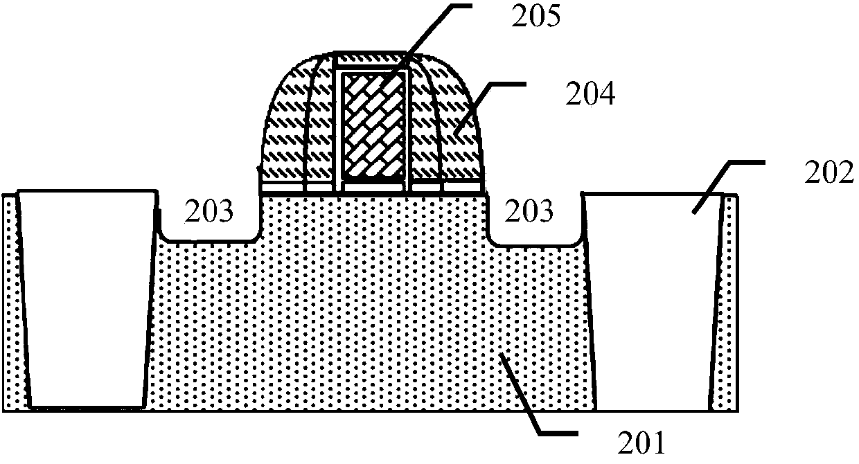
[0044] Step S01, such as Figure 5a As shown, an N-type wafer silicon substrate 301 formed with a gate 304 is provided. The gate 304 is protected by a sacrificial layer, and the silicon substrate 301 between the gate 304 and the shallow trench isolation STI302 is etched to be Form the groove 303 of source / drain region; Wherein, the depth of groove 303 is
[0045] Step S02, such as Figure 5b As shown, a low-temperature epitaxy method is used to deposit a first buffer layer (SiGe film) 305 in the groove 303; wherein, the first buffer layer contains a Ge concentration of 20% and a thickness of
[0046] Step S03, such as Figure 5c As shown, the low temperature epitaxy method is used to deposit the first bulk layer (SiGe thin film) 306 on the first buffer layer 305; wherein, the first bulk layer contains Ge concentration ...
no. 3 example
[0063] The method for manufacturing the SiGe source / drain region of this embodiment includes the following steps:
[0064] Step S01, providing an N-type wafer silicon substrate formed with a gate, the gate is protected by a sacrificial layer, and etching a source / drain region to be formed on the silicon substrate between the gate and the shallow trench isolation STI groove; where the depth of the groove is
[0065] Step S02, using a low-temperature epitaxy method to deposit a first buffer layer in the groove; wherein, the first buffer layer contains a Ge concentration of 15% and a thickness of The epitaxy temperature is 720°C;
[0066] Step S03, using a low-temperature epitaxy method to deposit a first body layer on the first buffer layer; wherein, the first body layer contains a Ge concentration of 35% and a thickness of B doping concentration 1e 19 cm -3 , the epitaxy temperature is 640°C;
[0067] Step S04, using a low-temperature epitaxy method to deposit a seco...
PUM
 Abstract
Description
Claims
Application Information