
Field stop type insulated gate bipolar transistor manufacturing method

A bipolar transistor, insulated gate technology, applied in transistors, semiconductor/solid-state device manufacturing, semiconductor devices, etc., can solve the problems of long production cycle, high development cost, affecting device performance, etc.

Inactive Publication Date: 2014-12-31
CSMC TECH FAB2 CO LTD
View PDF6 Cites 3 Cited by
  • Summary
  • Abstract
  • Description
  • Claims
  • Application Information

AI Technical Summary

Problems solved by technology

Due to the protection of the front structure, the annealing temperature should not be too high. At this time, the impurity activation rate is very low, which affects the device performance.
Moreover, the ion implantation method on the back side cannot push the impurities into the deep layer, and can only obtain a thinner FS layer on the back side, which will affect the performance of the device.
There is also a method of forming a field stop layer by long-term diffusion and well pushing, and then epitaxially growing a voltage-resistant layer, but this method has a long production cycle, unsatisfactory concentration distribution, large concentration gradient, and difficulty in controlling the thinning thickness
Moreover, the above-mentioned backside ion implantation and laser annealing processes also require relatively expensive high-energy ion implantation equipment and laser annealing equipment, and the development cost is relatively large.

Method used


Image

  • Field stop type insulated gate bipolar transistor manufacturing method
  • Field stop type insulated gate bipolar transistor manufacturing method

Examples


Embodiment Construction

[0027] The specific implementation manners of the present invention will be described in detail below in conjunction with the accompanying drawings.

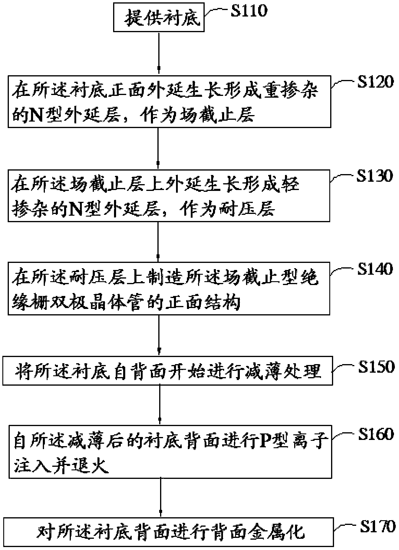
[0028] figure 1 It is a flowchart of an embodiment of the present invention, including:

[0029] Step S110: providing a substrate.

[0030] Choose a suitable type of substrate, either P-type or N-type. Because the substrate will eventually be thinned and cut off, the choice is relatively free and a lower-cost substrate can be selected. The substrate resistivity depends on the requirements of different IGBT products, the resistivity ranges from 0.001 to 200 ohm·m, and the substrate thickness ranges from 100 to 1000 microns.

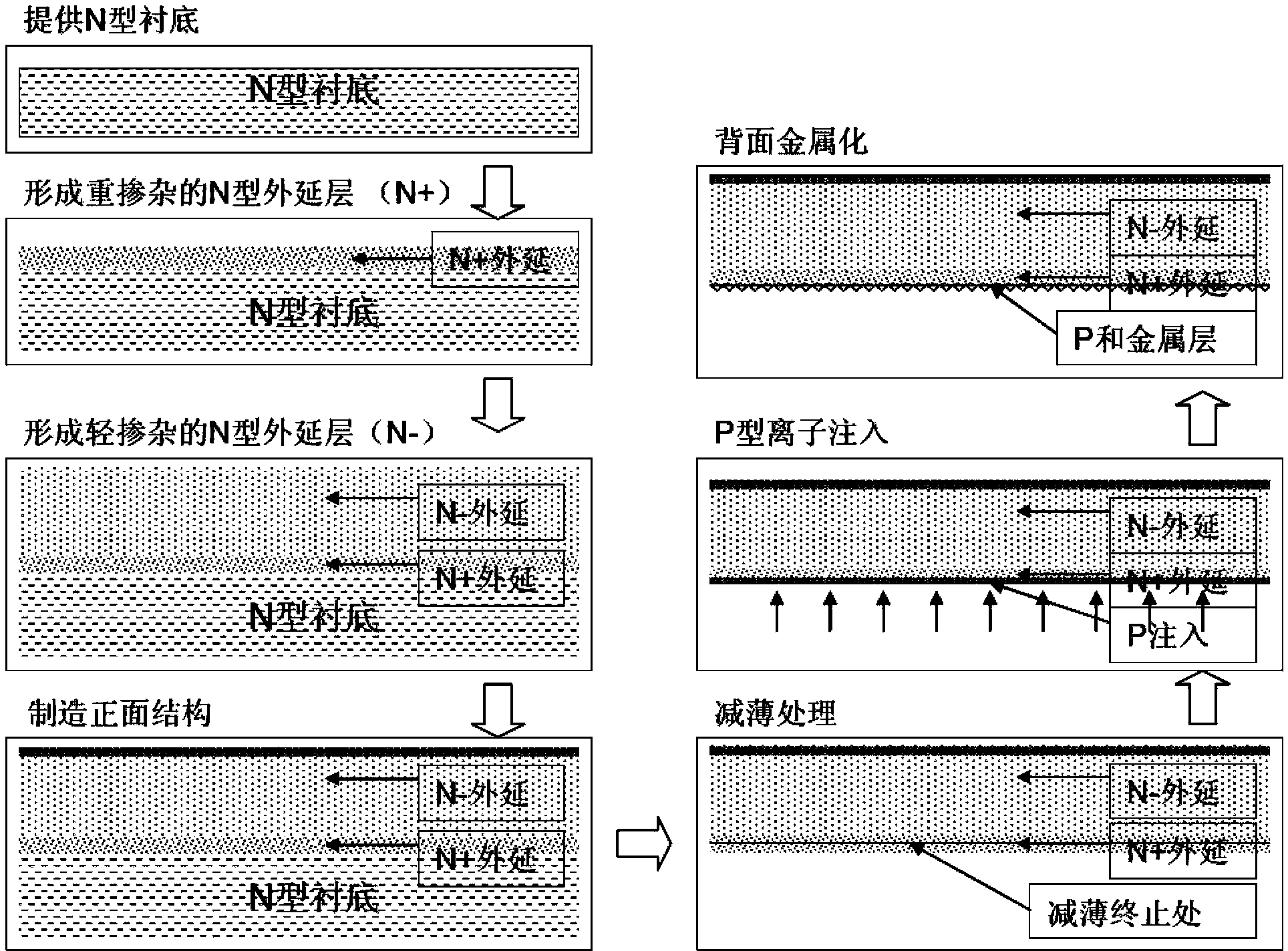
[0031] Step S120: epitaxially growing a heavily doped N-type epitaxial layer (N+) on the front side of the substrate as a field stop layer.

[0032] Vapor phase epitaxy is used to epitaxially grow a heavily doped N-type epitaxial layer as a field stop layer. The thickness and resistivity of the field sto...


PUM

PropertyMeasurementUnit
Thicknessaaaaaaaaaa
Thicknessaaaaaaaaaa

Abstract

The invention discloses a field stop type insulated gate bipolar transistor manufacturing method. The method includes epitaxially growing and generating heavily doped N-type epitaxial layer on a substrate as a field stop layer, then epitaxially growing and generating slightly doped N-type epitaxial layer as a pressure resistant layer, performing the conventional front process, then perform back thinning process, injecting P-type impurity into the back and annealing to obtain a P-type collector area, and performing the conventional back metallizing process. The method has the advantages that the producing period is short, expensive high-energy ion injection equipment and laser annealing equipment are omitted, the thickness of the field stop layer and the concentration of the impurity can be controlled according to component requirements, the thinning process difficulty is reduced, the component performance is improved, and the process difficulty is lowered; the substrate can be selected freely, and the substrate with lower cost can be selected.

Description

technical field [0001] The invention relates to the technical field of semiconductor devices, in particular to a preparation method of a field stop type insulated gate bipolar transistor. Background technique [0002] Insulated Gate Bipolar Transistor (Insulated Gate Bipolar Transistor, IGBT) is a new type of composite device that combines the advantages of power field effect transistors and power transistors. The transistor's low saturation voltage characteristics and the ability to easily realize a large current not only have the advantages of high input impedance, fast working speed, good thermal stability and simple driving circuit, but also have low on-state voltage, high withstand voltage and large current. The advantages, which make IGBT become a particularly attractive power electronics drive device in the field of power electronics in recent years, and have been more and more widely used. [0003] The development of IGBT has mainly experienced three types: punch-th...

Claims


Application Information

Patent Timeline
IPC IPC(8): H01L21/331
CPCH01L29/66333H01L29/7395
Inventor 王万礼邓小社王根毅芮强
Owner CSMC TECH FAB2 CO LTD
Learn More