Intermediate connecting layer of organic tandem solar cell and high-efficiency solar cell
A stacked cell and solar cell technology, applied in circuits, photovoltaic power generation, electrical components, etc., can solve the problems of unreachable, lack, high photoelectric conversion efficiency, etc., and achieve the effect of improving the utilization rate
- Summary
- Abstract
- Description
- Claims
- Application Information
AI Technical Summary
Problems solved by technology
Method used
Image
Examples
Embodiment 1
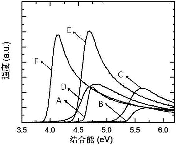
[0042] 10 nm molybdenum oxide and 12 nm silver were deposited on an ITO glass substrate. A 10 nm thin film of PFN was subsequently spin-coated. The structure has good electrical characteristics, the sheet resistance is 8Ω / □, and the work function is shown in figure 2 .
[0043] figure 2 Among them, A represents the ITO substrate, B represents the deposition of 10nm molybdenum oxide on the ITO substrate, C represents the deposition of 10nm molybdenum oxide and 14nm silver on the ITO substrate, D represents the deposition of 10nm molybdenum oxide, 14nm silver and 10nm PFN on the ITO substrate, E represents the deposition of 10nm oxide on the ITO substrate Molybdenum and 10nm PFN, F means 10nm PFN film deposited on ITO substrate. It can be seen that the two sides of the intermediate connection layer have different work functions, and can form good hole and electron ohmic contacts with the front sub-cell and the back sub-cell respectively, thereby forming a good connection. ...
Embodiment 2
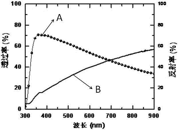
[0045] Deposit 10nm molybdenum oxide, 12nm silver and 10nm PFN film on glass substrate, the structure is reflective, its optical properties are as image 3 As shown, A represents the transmittance curve, and B represents the reflectance curve. It can be seen that the intermediate connection layer has strong reflectivity, and at the same time, the light loss caused by the intrinsic absorption of the intermediate connection layer is very weak. This shows that the intermediate layer has the possibility of modulating the light field distribution in the device, and at the same time, the intermediate connection layer can be used in the device as an effective connection layer.
Embodiment 3
[0047] The glass substrate covered with ITO was ultrasonically washed with detergent, isopropanol, ethanol, and acetone for 15 minutes in sequence, and after being treated with ultraviolet-ozone, a zinc oxide electron transport layer with a thickness of 20-40nm was prepared by solution spin coating. Then spin-coat benzodiindenethiophene-quinoxaline alternating copolymer (PIDT-PhanQ) of about 60nm on it: PC 71 BM photosensitive layer and annealed on a hot stage at 120 °C for 5 min to form the front subcell.
[0048] Deposit molybdenum oxide of about 10nm and silver of 4nm, and then spin-coat a PFN film of about 10nm to form an intermediate connection layer.
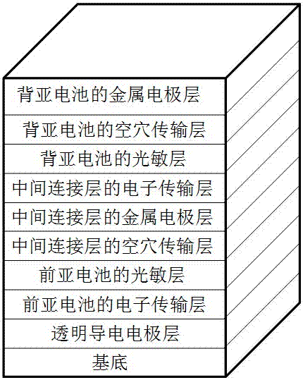
[0049] Finally spin coat 80nm PTB-7:PC 71 BM thin film photosensitive layer, deposit 10nm molybdenum oxide hole transport layer and 100nm silver electrode to form the back sub-cell. get as figure 1 The shown organic tandem solar cell has a photoelectric conversion efficiency of 8.6%.
PUM
 Abstract
Description
Claims
Application Information


