

Method for improving thickness homogeneity of silicon extending slices for CCD device
A silicon epitaxial wafer with uniform thickness technology, applied in semiconductor/solid-state device manufacturing, electrical components, circuits, etc., can solve problems such as difficult to meet the requirements of CCD devices, and achieve the goal of advancing the development process, meeting high performance, and improving thickness uniformity Effect
- Summary
- Abstract
- Description
- Claims
- Application Information
AI Technical Summary
Problems solved by technology
Method used
Image

Examples
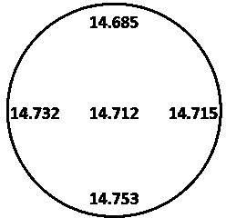
Embodiment 1
[0021] (1) First use HCl gas to etch the base of the epitaxial furnace to remove the residual deposits on the base. The corrosion temperature is set at 1150°C, the purity of HCl gas is ≥99.99%, the flow rate is set at 3L / min, and the corrosion The time is set at 5 minutes, and then the base is re-coated with a layer of intrinsic polysilicon. The raw material for polysilicon growth is trichlorosilane gas with a purity of ≥99.95%. The flow rate is set at 30g / min, and the polysilicon growth time is set at 15 minutes.
[0022] (2) Put a monocrystalline silicon substrate into the pit of the base. The conductivity type of the silicon substrate is P type, polished on one side, the crystal orientation is ±0.5°, the resistivity is 0.01Ω?cm, and the thickness is 450 μm and a diameter of 100 mm. Nitrogen and hydrogen are used to purge the reaction chamber of the epitaxial furnace, the purity of nitrogen and hydrogen are both ≥99.999%, the purge gas flow rate is set to 100L / min, and the p...
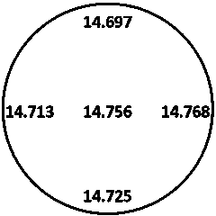
Embodiment 2
[0030] (1) Use HCl gas to corrode the base of the epitaxial furnace to remove the residual deposits on the base. The corrosion temperature is set at 1160°C, the purity of HCl gas is ≥99.99%, the flow rate is set at 3L / min, and the corrosion time is Set it to 5 minutes, and then re-wrap the base with a layer of intrinsic polysilicon. The raw material for polysilicon growth is trichlorosilane gas with a purity of ≥99.95%. The flow rate is set to 30g / min, and the polysilicon growth time is set to 15 minutes.
[0031] (2) Put a monocrystalline silicon substrate into the pit of the base. The conductivity type of the silicon substrate is P type, polished on one side, the crystal orientation is ±0.5°, the resistivity is 0.01Ω?cm, and the thickness is 450 μm and a diameter of 100 mm. Nitrogen and hydrogen are used to purge the reaction chamber of the epitaxial furnace, the purity of nitrogen and hydrogen are both ≥99.999%, the flow rate of purge gas is set to 100L / min, and the purge t...
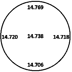
Embodiment 3
[0039] (1) First use HCl gas to etch the base of the epitaxial furnace to remove the residual deposits on the base. The corrosion temperature is set at 1180°C, the purity of HCl gas is ≥99.99%, the flow rate is set at 3L / min, and the corrosion The time is set at 5 minutes, and then the base is re-coated with a layer of intrinsic polysilicon, and the raw material for polysilicon growth is trichlorosilane (SiHCl 3 ) gas with a purity of ≥99.95%, the flow rate is set to 30g / min, and the polysilicon growth time is set to 15min.
[0040] (2) Put a monocrystalline silicon substrate into the pit of the base. The conductivity type of the silicon substrate is P type, polished on one side, the crystal orientation is ±0.5°, the resistivity is 0.01Ω?cm, and the thickness is 450 μm and a diameter of 100 mm. Nitrogen and hydrogen are used to purge the reaction chamber of the epitaxial furnace, the purity of nitrogen and hydrogen are both ≥99.999%, the purge gas flow rate is set to 100L / min...
PUM
| Property | Measurement | Unit |
|---|---|---|
| thickness | aaaaa | aaaaa |
| diameter | aaaaa | aaaaa |
Abstract
Description
Claims
Application Information