Method for packaging Ni-P substrate

A packaging method and substrate technology, which is applied in the manufacture of electrical components, electrical solid devices, semiconductor/solid devices, etc., can solve the problems of large substrate resin damage, limitation, and long processing time, and achieve low cost, suppress delamination, and reduce The effect of growth rate

Active Publication Date: 2015-01-14
CENT SOUTH UNIV
View PDF4 Cites 5 Cited by
  • Summary
  • Abstract
  • Description
  • Claims
  • Application Information

AI Technical Summary

Problems solved by technology

However, vacuum heat treatment has higher requirements on equipment, longer processing time, greater damage to substrate resin, and limited application
[0004] In addition, despite the strong magnetic field (1-12×10 4 G) Coupled reflow soldering technology has been reported in some literature, but the use of strong magnetic field will have adverse effects such as magnetization and degaussing on the packaged magnetic chip, etc., and the reflow soldering technology using weak magnetic field with nano-nickel powder is still in the packaging field. No related reports

Method used


Image

  • Method for packaging Ni-P substrate
  • Method for packaging Ni-P substrate
  • Method for packaging Ni-P substrate

Examples


Embodiment 1

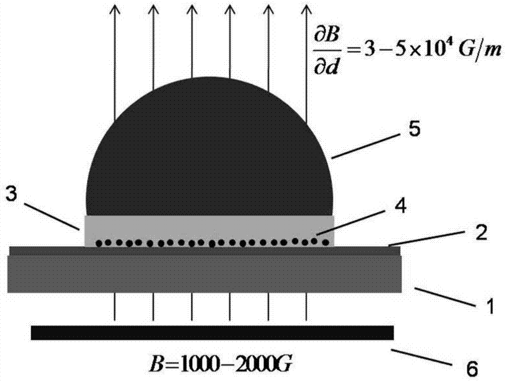
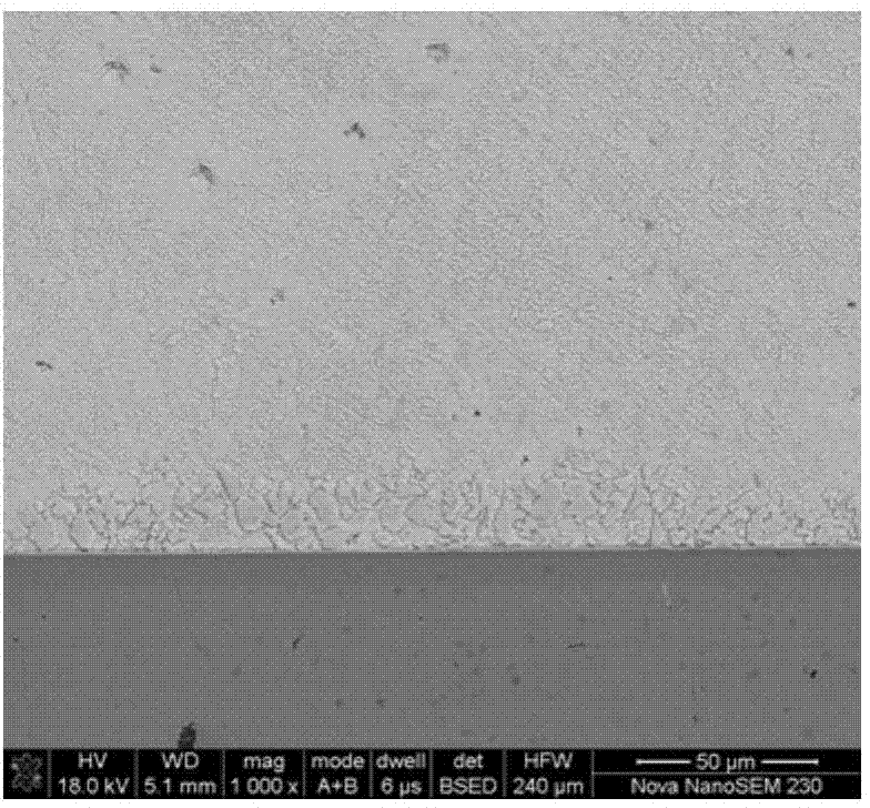
[0048] Precisely prepare nano-nickel powder (particle size range 80-100nm) mass percentage is 5%, no-cleaning flux mass percentage is 95% mixed flux; -2 Pa) Stirring for 1h at a stirring speed of 200r / min to obtain a mixed flux containing nano-Ni powder that is uniformly mixed; before packaging, uniformly print a layer of mixed flux with a thickness of 15 μm on a Ni-P plate with a thickness of 10 μm, Then print a Sn-3.5Ag (wt.%) solder paste with a thickness of 400 μm on the Ni-P substrate; place the Ni-P substrate in a magnetic induction gradient of 3×10 4 G / m, the magnetic field source is located inside the substrate, and in a magnetic field with a magnetic induction intensity of 1000G at the welding interface, the welding atmosphere is 99.99% high-purity nitrogen, the airflow rate is 1500ml / min, and the heating rate during reflow soldering is 5°C / s. Activate at 160°C for 10s, reach a peak temperature of 250°C, reflow at the peak temperature for 120s, and cool to room temper...

Embodiment 2

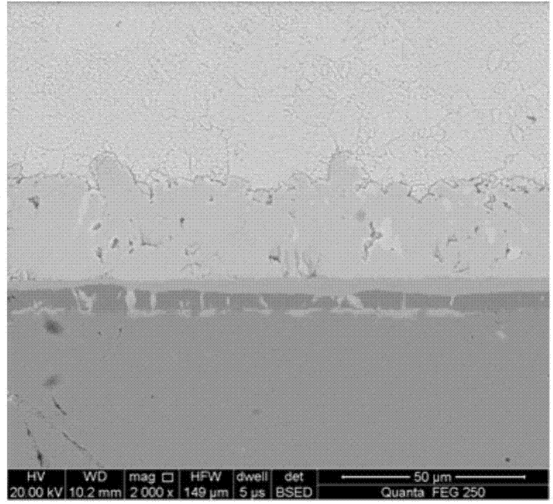
[0051] Accurately prepare nickel powder (particle size range 60-100nm) mass percentage is 15%, no-cleaning flux mass percentage is 85% mixed flux; -2 Pa), stirred at a stirring speed of 150r / min for 1h to obtain a mixed flux containing nano-Ni powder; before packaging, evenly print a layer of mixed flux with a thickness of 10 μm on a Ni-P plate with a thickness of 10 μm , and then print Sn-3.5Ag (wt.%) solder paste with a thickness of 500 μm on the Ni-P substrate; place the Ni-P substrate in a magnetic induction gradient of 5×10 4 G / m, the magnetic field source is located inside the substrate, and in a magnetic field with a magnetic induction intensity of 2000G at the welding interface, the welding atmosphere is 99.99% high-purity nitrogen, the airflow rate is 2000ml / min, and the heating rate during reflow soldering is 10°C / s. Activate at 180°C for 10s, reach a peak temperature of 250°C, reflow at the peak temperature for 120s, and cool to room temperature at a cooling rate of...

Embodiment 3

[0054] Accurately prepare nickel powder (particle size range 50-80nm) mass percentage is 10%, no-clean flux mass percentage is 90% mixed flux; in a mixer (vacuum degree 1.5 × 10 -2 Pa), stirred at a stirring speed of 300r / min for 0.5h to obtain a mixed flux containing nano-Ni powder mixed uniformly; before packaging, uniformly print a layer of mixed flux with a thickness of 10 μm on a Ni-P plate with a thickness of 10 μm flux, and then print a thickness of 500 μm Sn-3.5Ag (wt.%) solder paste on the Ni-P substrate; the Ni-P substrate is placed in a magnetic induction gradient of 4 × 10 4 G / m, the magnetic field source is located inside the substrate, and in a magnetic field with a magnetic induction intensity of 1500G at the welding interface, the welding atmosphere is 99.99% high-purity nitrogen, the airflow rate is 3000ml / min, and the heating rate during reflow soldering is 8°C / s. Activate at 160°C for 15s, reach a peak temperature of 250°C, reflow at the peak temperature for...


PUM

PropertyMeasurementUnit
particle sizeaaaaaaaaaa
thicknessaaaaaaaaaa
thicknessaaaaaaaaaa

Abstract

The invention relates to a method for packaging a Ni-P substrate and belongs to the technical field of electronic packaging. According to the method for packaging the Ni-P substrate, after 5-20 wt % of nano nickel powder and 80-95 wt % of scaling powder are evenly mixed, an Ni-P substrate is coated or printed with the mixture and then is coated or printed with tin-based solder, and then the substrate to be welded is obtained; the substrate to be welded is placed in a static magnetic field, and then reflow soldering is conducted, wherein the gradient of the intensity of the static magnetic field is 3-5*104 G/m, the magnetic induction intensity of the position where the substrate is located ranges from 1000 G to 2000 G, and the magnetic field source is located on the inner side of the Ni-P substrate. According to the method for packaging the Ni-P substrate, the Ni-P wear rate is greatly reduced when welding points are on service, growth of intermetallic compounds is restrained, and layering or stripping of the interface intermetallic compounds is also avoided; the reliability of the welding points is higher, cost is low, production efficiency is high, the technical stability is excellent, and the method is suitable for large-scale industrial application.

Description

technical field [0001] The invention relates to a Ni-P substrate packaging method; in particular to a method for suppressing Ni-P layer consumption and interface layer intermetallic compound growth and packaging the Ni-P substrate with tin-containing solder; it belongs to the technical field of electronic packaging. Background technique [0002] The amorphous electroless Ni-P layer with a P mass percentage of 6-9% has good adhesion to most substrates (copper plates, silicon plates, etc.), and can effectively prevent Sn in the tin-based solder from interacting with the substrate. Reaction. Compared with general metal and alloy coatings, amorphous Ni-P alloy has excellent mechanical properties and physical and chemical properties, such as high hardness, good wear resistance and corrosion resistance; in addition, it has good reliability Solderability, thickness uniformity and controllability, bright and beautiful surface, therefore, amorphous Ni-P electroless coating is used a...

Claims


Application Information

Patent Timeline
Patent Type & Authority Applications(China)
IPC IPC(8): H01L21/60H01L21/56
CPCH01L24/27H01L24/29H01L2224/27H01L2924/0132
Inventor 马运柱刘文胜王依锴黄宇峰
Owner CENT SOUTH UNIV
Why Eureka
Try Eureka