Homogeneous epitaxial growth method on GaN (gallium nitride) substrate

A homoepitaxial and epitaxial growth technology, which is applied in semiconductor/solid-state device testing/measurement, coating, gaseous chemical plating, etc., can solve the problems of not getting the expected device performance and improvement, and increase the internal quantum recombination efficiency and Effects of external quantum emission efficiency, heat generation reduction, and dislocation density reduction

Active Publication Date: 2015-02-11
PEKING UNIV
View PDF4 Cites 7 Cited by
  • Summary
  • Abstract
  • Description
  • Claims
  • Application Information

AI Technical Summary

Problems solved by technology

[0005] This is very different from the substrates used in the first and second generation semiconductor devices, such as Si, GaAs, InP, etc. As a result, devices grown epitaxially on HVPE GaN s

Method used


Image

  • Homogeneous epitaxial growth method on GaN (gallium nitride) substrate
  • Homogeneous epitaxial growth method on GaN (gallium nitride) substrate
  • Homogeneous epitaxial growth method on GaN (gallium nitride) substrate

Examples


Embodiment 1

[0036] Example 1: Homoepitaxial growth on c-plane self-supporting GaN substrate

[0037] Include the following steps:

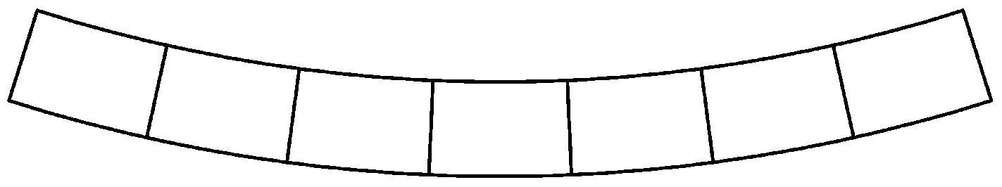
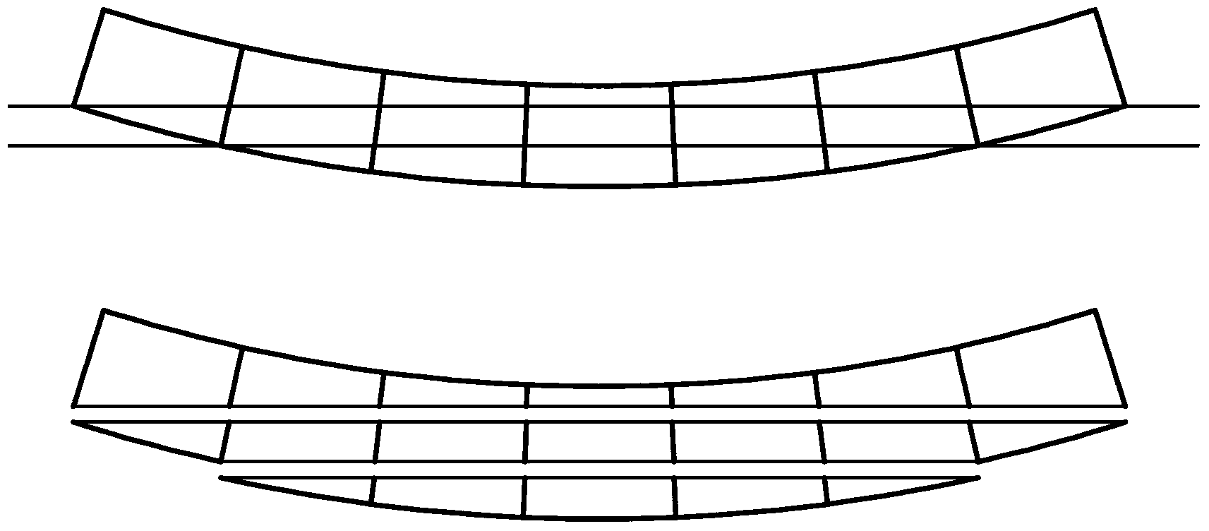
[0038] 1) The GaN substrate is grown by HVPE method. After cleaning, the radius of curvature of the surface is measured. In this embodiment, the thickness of the sample is 2000 μm, and the radius of curvature is 10 meters.

[0039] 2) A relatively flat GaN substrate is obtained by chemical mechanical polishing (CMP), and a silicon dioxide mask layer with a thickness of 100 nm is deposited by PECVD.

[0040] 3) Concentric mask rings with a width of 1-20 μm are formed by using a conventional semiconductor photolithography process; the pitch of the concentric rings is 1-100 μm.

[0041] 4) After cleaning, put it into MOCVD for growth. The growth process uses nitrogen, hydrogen or a mixture of the two as the carrier gas. The temperature of the epitaxial GaN layer is 900°C-1200°C, and the pressure is 100-500Torr. In this embodiment, the obtained GaN epitaxial la...

Embodiment 2

[0043] Embodiment two: the growth based on the light-emitting diode (LED) of embodiment one

[0044] A conventional semiconductor photolithography process is used to form concentric mask rings with a width of 1 μm, and the pitch of the concentric rings is 1 μm. After cleaning, it is placed in MOCVD for growth. The growth process uses nitrogen and hydrogen as carrier gases. The temperature of the epitaxial GaN layer is 900°C-1200°C, the pressure is 100-500Torr, and the thickness of the growth surface is 5μm. Use the 5μm thick GaN epitaxial wafer grown by MOCVD as the substrate, and continue to grow light-emitting diodes (LEDs) by MOCVD. Due to the modulated growth of the annular mask, a light-emitting diode with an increase in light extraction efficiency of more than 50% can be obtained .

Embodiment 3

[0045] Embodiment three: the growth based on the light-emitting diode (LED) of embodiment one

[0046] A conventional semiconductor photolithography process is used to form concentric mask rings with a width of 1 μm and a pitch of 100 μm. After cleaning, it is placed in MOCVD for growth. The growth process uses nitrogen and hydrogen as carrier gases. The temperature of the epitaxial GaN layer is 900°C-1200°C, the pressure is 100-500Torr, and the thickness of the growth surface is 5μm. Using the 5μm thick GaN epitaxial wafer grown by MOCVD as the substrate, and continuing to grow light-emitting diodes (LEDs) by MOCVD, the light extraction efficiency can be increased by more than 50% due to the modulated growth of the ring mask. led.


PUM

PropertyMeasurementUnit
Thicknessaaaaaaaaaa
Thicknessaaaaaaaaaa

Abstract

The invention discloses a homogeneous epitaxial growth method on a GaN (gallium nitride) substrate. The homogeneous epitaxial growth on the GaN substrate is realized through the lateral epitaxy of an annular pattern mask. The method has the advantages that a perfect GaN epitaxy layer can be obtained, the dislocation density can be effectively reduced, the dislocation density of the epitaxy layer can reach a value lower than 106/cm<2>, the piezoelectric polarization effect of a GaN-based LED (light emitting diode) can be effectively reduced, the inner quantum compounding efficiency and the outer quantum emitting efficiency can be improved, the integral light outlet efficiency can reach more than 1.5 times of that of an ordinary LED, the heating quantity of a device can be effectively reduced, and the service life of the device can be prolonged.

Description

technical field [0001] The invention belongs to the technical field of semiconductor optoelectronics, relates to the field of epitaxial growth of thin films of semiconductor materials and the technical field of metal organic compound chemical vapor deposition (MOCVD), in particular to a gallium nitride (GaN) substrate realized by lateral epitaxy using a ring pattern mask The method of homoepitaxial growth. Background technique [0002] Nitride semiconductor materials represented by GaN, InN, AlN and their ternary and quaternary systems have a direct band gap and a continuously variable bandwidth from 0.7eV to 6.2eV. Its excellent physical and chemical stability, high saturation electron mobility and other characteristics make it the preferred material for GaN-based lasers, light-emitting diodes and other optoelectronic devices. [0003] Currently widely used sapphire (Sapphire) or silicon carbide (SiC) substrates and gallium nitride (GaN) materials have large lattice mismat...

Claims


Application Information

Patent Timeline
IPC IPC(8): H01L21/02H01L21/66C23C16/44
CPCC23C16/44C23C16/52H01L21/0262H01L21/02634
Inventor 杨志坚秦志新于彤军吴洁君胡晓东康香宁王新强许福军沈波张国义
Owner PEKING UNIV
Why Eureka
Try Eureka