A double-layer structure window layer applied to high-efficiency thin-film photovoltaic cells

A double-layer structure and window layer technology, applied in circuits, electrical components, sustainable manufacturing/processing, etc., can solve the problems of increasing photogenerated electron-hole recombination, low conversion efficiency, reducing device open circuit voltage and fill factor, etc.

Active Publication Date: 2016-10-05
苏州柯利达集团有限公司
View PDF4 Cites 0 Cited by
  • Summary
  • Abstract
  • Description
  • Claims
  • Application Information

AI Technical Summary

Problems solved by technology

However, the conversion efficiency of thin-film photovoltaic devices is generally lower than that of silicon-based devices. In order to further improve the energy conversion efficiency of thin-film photovoltaic technology, reduce production costs, and enhance its market competitiveness, optimize each functional layer and improve the interface. Performance is a very important way
Taking copper indium gallium selenide as an example, vacuum sputtering technology is used in traditional battery devices to prepare zinc oxide window layers. Due to the bombardment and damage of high-energy ions to the surface of the functional layer below during the sputtering process, a large number of particles will be generated at the interface of the functional layer. The defect state increases the recombination of photogenerated electron holes, thereby reducing the open circuit voltage and fill factor of the device

Method used


Image

  • A double-layer structure window layer applied to high-efficiency thin-film photovoltaic cells
  • A double-layer structure window layer applied to high-efficiency thin-film photovoltaic cells

Examples


Embodiment Construction

[0019] Preferred embodiments of the present invention will be described in detail below in conjunction with the accompanying drawings.

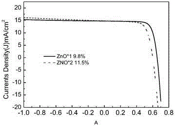
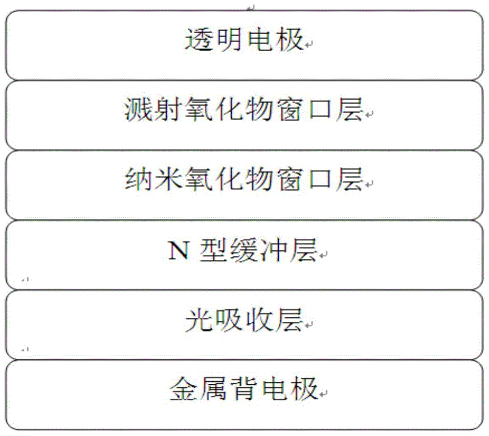
[0020] Such as figure 1 As shown, it is a structural schematic diagram of a copper indium gallium selenide photovoltaic device using a double-layer structure window layer. The device comprises: a metal back electrode 1; a copper indium gallium selenide light absorbing layer 2; an N-type buffer layer 3; a double-layer structure window layer 4, the window layer includes a nano-zinc oxide layer prepared by a solution method and a high-density zinc oxide layer prepared by a vacuum sputtering method. a dense zinc oxide layer; and a transparent conductive substrate 5 .

[0021] The metal back electrode 1 is generally aluminum, but not limited thereto, and also includes gold, silver, copper, titanium, chromium, molybdenum and other metals. Above the metal electrode 1 is a light absorbing layer 2 with a thickness between 0.1-10um, made of lead sele...


PUM

PropertyMeasurementUnit
thicknessaaaaaaaaaa
thicknessaaaaaaaaaa
thicknessaaaaaaaaaa

Abstract

The invention discloses a bilayer structure window layer applied to an efficient thin-film photocell. The bilayer structure window layer comprises nano metal oxide prepared by a solution method and a metal oxide layer prepared by a vacuum sputtering method. The bilayer structure window layer maintains high compactness of an oxide thin film prepared by the vacuum sputtering method, and the nano metal oxide thin film is prepared through the solution method, so that damage to the surfaces of other functional layers in the process of vacuum sputtering is avoided, interface composition is effectively reduced, and FF and open-circuit voltage of the photocell are increased. Compared with a device taking a monolayer nano metal oxide or the oxide thin film prepared through vacuum sputtering as a window layer, the bilayer structure window layer has the advantage that conversion efficiency of the thin-film photocell based on the bilayer structure window layer is improved by more than 15%.

Description

technical field [0001] The invention belongs to the field of optoelectronic devices and relates to a new double-layer structure window layer applicable to high-efficiency thin-film photovoltaic cells. Background technique [0002] Compared with polycrystalline silicon and monocrystalline silicon photovoltaic cells, thin-film photovoltaic cells have the advantages of light weight, low production energy consumption, and higher light absorption, so they have attracted widespread attention. Thin-film photovoltaic cells mainly include the following categories according to light-absorbing materials: the first category, inorganic compound thin-film materials such as copper indium gallium selenide, copper zinc tin sulfur, and cadmium telluride. The second category, organic polymers and small organic molecules. The third category is organic-inorganic composite materials, such as perovskite-structured materials. The fourth category is quantum dot films based on inorganic nanomateria...

Claims


Application Information

Patent Timeline
Patent Type & Authority Patents(China)
IPC IPC(8): H01L31/0216H01L31/18
CPCH01L31/02167H01L31/18Y02P70/50
Inventor 钱磊章婷谢承智刘德昂
Owner 苏州柯利达集团有限公司
Why Eureka
Try Eureka