Insulated Gate Right Angle Composite Source Field Plate Power Transistor

A power transistor, insulated gate technology, applied in the field of microelectronics, can solve the problems of reducing the yield of the device, tedious process debugging, increasing the difficulty of the device, etc., and achieve the effects of improving reliability, reducing leakage current, and large drain-source voltage

Active Publication Date: 2017-04-19
陕西半导体先导技术中心有限公司
View PDF4 Cites 0 Cited by
  • Summary
  • Abstract
  • Description
  • Claims
  • Application Information

AI Technical Summary

Problems solved by technology

However, the process of GaN-based double-layer field plate HEMT devices is complex and the manufacturing cost is higher. The fabrication of each field plate requires process steps such as photolithography, metal deposition, and passivation dielectric deposition.
Moreover, in order to optimize the thickness of the dielectric material under the field plates of each layer to maximize the breakdown voltage, tedious process debugging and optimization must be carried out, which greatly increases the difficulty of device manufacturing and reduces the yield of devices.

Method used


Image

  • Insulated Gate Right Angle Composite Source Field Plate Power Transistor
  • Insulated Gate Right Angle Composite Source Field Plate Power Transistor
  • Insulated Gate Right Angle Composite Source Field Plate Power Transistor

Examples


Embodiment 1

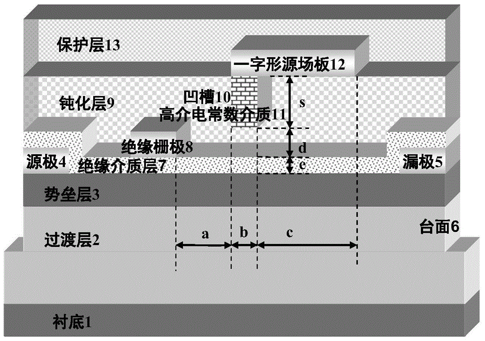
[0044] Embodiment 1: The production substrate is sapphire, and the insulating dielectric layer is SiO 2 , the passivation layer is Al 2 o 3 , the protective layer is SiN, and the high dielectric constant dielectric is HfO 2 , the insulated gate right-angle compound source field plate power transistor with the inline source field plate as Ti / Mo / Au metal combination.

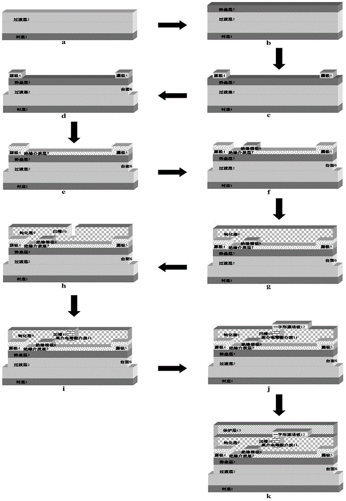
[0045] Step 1. On the sapphire substrate 1, make the transition layer 2 by epitaxial GaN material from bottom to top, such as image 3 a.

[0046] An undoped transition layer 2 with a thickness of 1 μm is epitaxially formed on the sapphire substrate 1 by metal organic chemical vapor deposition technology, and the transition layer is composed of GaN materials with thicknesses of 30 nm and 0.97 μm from bottom to top. The process conditions used for the epitaxial lower GaN material are: temperature 530°C, pressure 45 Torr, hydrogen gas flow rate 4400 sccm, ammonia gas flow rate 4400 sccm, gallium source flow rate...

Embodiment 2

[0067] Embodiment 2: The substrate is made of silicon carbide, and the insulating dielectric layer is HfO 2 , the passivation layer is SiN, the protective layer is SiO 2 , the high dielectric constant dielectric is Al 2 o 3 , the insulated gate right-angle composite source-field-plate power transistor with the in-line source-field plate as Ti / Ni / Au metal combination.

[0068] Step 1. Epitaxially AlN and GaN materials on the silicon carbide substrate 1 to form the transition layer 2, such as image 3 a.

[0069] 1.1) Using metal-organic chemical vapor deposition technology to epitaxially undoped AlN material with a thickness of 50nm on the silicon carbide substrate 1; the process conditions for the epitaxy are: temperature is 1000°C, pressure is 45Torr, hydrogen flow rate is 4600sccm, The flow rate of ammonia gas is 4600 sccm, and the flow rate of aluminum source is 5 μmol / min;

[0070] 1.2) Using metal-organic chemical vapor deposition technology to epitaxially GaN materi...

Embodiment 3

[0104] Embodiment three: making substrate is silicon, insulating dielectric layer is Al 2 o 3 , the passivation layer is SiO 2 , the protective layer is SiN, and the high dielectric constant dielectric is HfO 2 , the insulated-gate right-angle composite source-field-plate power transistor with the in-line source-field plate as Ti / Pt / Au metal combination.

[0105] Step A. Epitaxial AlN and GaN materials on the silicon substrate 1 from bottom to top to make the transition layer 2, such as image 3 a.

[0106] A1) Using metal-organic chemical vapor deposition technology at a temperature of 800° C., a pressure of 40 Torr, a flow rate of hydrogen gas of 4000 sccm, a flow rate of ammonia gas of 4000 sccm, and a flow rate of aluminum source of 25 μmol / min, the epitaxy on the silicon substrate 1 AlN material with a thickness of 200nm;

[0107] A2) Using metal-organic chemical vapor deposition technology at a temperature of 980°C, a pressure of 45 Torr, a flow rate of hydrogen gas...


PUM


Abstract

The invention discloses an insulated gate type power transistor of a right-angled composite source field plate. The insulated gate type power transistor is mainly used for solving the problem that the process for realizing high breakdown voltage is complex in the existing field plate technology. The insulated gate type power transistor of the right-angled composite source field plate comprises a substrate (1), a transition layer (2), a barrier layer (3), a source electrode (4), a drain electrode (5), a table board (6), an insulated medium layer (7), an insulated gate electrode (8), a passivation layer (8) and a protective layer (13), wherein a groove (10) is etched in the passivation layer (9); a high dielectric constant medium (11) is completely filled in the groove (10); a straight source field plate (12) is deposited between the passivation layer (9) and the protective layer (13); the straight source field plate is lean against one side edge of the insulated grid electrode and aligned with one side edge, close to the insulated gird plate, of the groove, and the straight source field plate is electrically connected with the source electrode; and the straight source field plate and the high dielectric constant medium form the right-angled composite source field plate. The insulated gate type power transistor of the right-angled composite source field plate has the advantages of a simple process, high breakdown voltage, high reliability and high yield.

Description

technical field [0001] The invention belongs to the technical field of microelectronics, and relates to a semiconductor device, in particular to an insulated gate type right-angle composite source field plate power transistor, which can be used as a basic device of a power electronic system. [0002] technical background [0003] Power semiconductor devices are important components of power electronic systems and effective tools for power processing. In recent years, as energy and environmental issues have become increasingly prominent, research and development of new high-performance, low-loss power devices has become one of the effective ways to improve power utilization, save energy, and alleviate energy crises. However, in the research of power devices, there is a serious constraint relationship between high speed, high voltage and low on-resistance. Reasonable and effective improvement of this constraint relationship is the key to improving the overall performance of the...

Claims


Application Information

Patent Timeline
Patent Type & Authority Patents(China)
IPC IPC(8): H01L29/40H01L29/778H01L21/335
CPCH01L29/402H01L29/66409H01L29/778
Inventor 毛维范举胜杨翠张昊赵雁鹏马晓华郝跃
Owner 陕西半导体先导技术中心有限公司
Why Eureka
Try Eureka