Growing method of light-emitting diode epitaxial wafer and light emitting diode epitaxial wafer

A technology for light emitting diodes and a growth method, which is applied in the field of light emitting diode epitaxial wafers, can solve the problems of little room for improving the luminous efficiency of the chip, cannot effectively improve the luminous efficiency of the chip, and increase the damage of the InGaN active layer, so as to avoid the working voltage. Raise, improve antistatic ability and reverse breakdown ability, improve the effect of light extraction efficiency

Active Publication Date: 2015-03-25
HC SEMITEK SUZHOU
View PDF4 Cites 10 Cited by
  • Summary
  • Abstract
  • Description
  • Claims
  • Application Information

AI Technical Summary

Problems solved by technology

[0005] Since the ionization rate of Mg in the P-type layer is very low, even if the doping concentration of Mg increases, the number of effective holes that the P-type layer can provide does not increase significantly, and even a self-compensation effect occurs, resulting in a decrease in luminous efficiency, etc. opposite effect
In addition, although the activation rate of Mg can be increased by increasing the growth temperature, the effective hole concentration of the P-type layer can be increased, but at the same time, the damage to the InGaN active layer will be increased.
Therefore, in the existing LED growth methods, the growth method of the P-type layer has little room for improving the luminous efficiency of the chip, and cannot effectively improve the luminous efficiency of the chip. Instead, the reverse breakdown voltage of the chip is reduced and the antistatic ability downside downside

Method used


Image

  • Growing method of light-emitting diode epitaxial wafer and light emitting diode epitaxial wafer
  • Growing method of light-emitting diode epitaxial wafer and light emitting diode epitaxial wafer

Examples


Embodiment 1

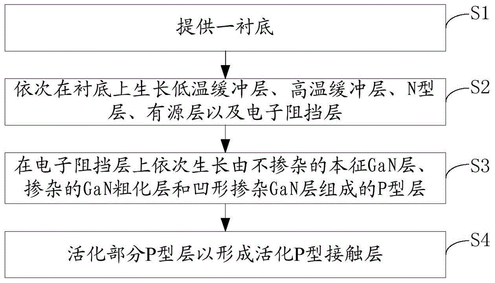
[0032] see figure 1 , an embodiment of the present invention provides a method for growing a light-emitting diode epitaxial wafer, the method comprising the following steps:

[0033] S1: providing a substrate;

[0034] Specifically, in this embodiment, the substrate may be sapphire. Before growing the epitaxial wafer, the substrate needs to be pretreated. The pretreatment operation includes: placing the substrate in a reaction chamber, and treating it at a high temperature under a hydrogen atmosphere. Substrate 5-6min. Wherein, the temperature of the reaction chamber is 1000-1100° C., and the pressure of the reaction chamber is controlled at 200-500 torr.

[0035] S2: growing a low-temperature buffer layer, a high-temperature buffer layer, an N-type layer, an active layer, and an electron blocking layer on the substrate in sequence;

[0036] Specifically, in this embodiment, Veeco K465i MOCVD (Metal Organic Chemical Vapor Deposition, Metal Organic Compound Chemical Vapor De...

Embodiment 2

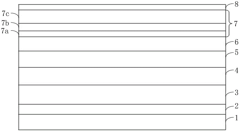
[0058] see figure 2 , the embodiment of the present invention provides a light-emitting diode epitaxial wafer, which is suitable for preparation by the method as in Example 1. The epitaxial wafer includes a substrate 1 and a low-temperature buffer layer 2, a high-temperature buffer layer 3, and N-type layer 4, active layer 5, electron blocking layer 6, P-type layer 7 and activated P-type contact layer 8, P-type layer 7 consists of undoped intrinsic GaN layer 7a, doped GaN rough layer 7b , concave-doped GaN layers 7c are sequentially stacked, the growth temperature of the concave-doped GaN layer 7c is higher than that of the intrinsic GaN layer 7a, and the growth temperature of the intrinsic GaN layer 7a is higher than that of the GaN roughened layer 7b,

[0059] The GaN rough layer 7b is doped with Mg of the first concentration, the concave doped GaN layer 7c is firstly doped with the second concentration of Mg, then with the third concentration of Mg, and finally with the fi...


PUM


Abstract

The invention discloses a growing method of a light-emitting diode epitaxial wafer, and belongs to the technical field of semiconductors. The growing method comprises the steps that a substrate is provided, and a low-temperature buffering layer, a high-temperature buffering layer, an N-type layer, an active layer and an electronic barrier layer grow on the substrate in sequence; a P-type layer composed of an undoped intrinsic GaN layer, a doped GaN armoring layer and a concave doped GaN layer grows, the growing temperature of the concave doped GaN layer is higher than that of the intrinsic GaN layer, the growing temperature of the intrinsic GaN layer is higher than that of the GaN armoring layer, first concentration Mg is used in the GaN armoring layer to carry out doping, second concentration Mg is adopted in the concave doped GaN layer to carry out doping, third concentration Mg is utilized for carrying out doping, finally the first concentration Mg is adopted to carry out doping, the first concentration is larger than the second concentration, and the second concentration is larger than the third concentration; the P-type layer is activated. The hole concentration is increased through high-temperature growing of the concave doped GaN layer, the Mg doping efficiency can be guaranteed, and damage to the InGaN active layer cannot be increased.

Description

technical field [0001] The invention relates to the technical field of semiconductors, in particular to a method for growing a light-emitting diode epitaxial wafer and the light-emitting diode epitaxial wafer. Background technique [0002] LED (Light Emitting Diode, light-emitting diode) is a semiconductor electronic component that can emit light. As a new type of solid-state lighting source with high efficiency, environmental protection and green, LED has low voltage, low power consumption, small size, light weight and long life. , high reliability and other advantages, are being rapidly and widely used, such as traffic lights, car interior and exterior lights, urban landscape lighting, mobile phone backlight, outdoor full-color display screens, etc., especially in the field of lighting, is still constantly seeking to improve chip luminous efficiency. [0003] The existing LED growth method includes: sequentially growing a low-temperature buffer layer, a high-temperature b...

Claims


Application Information

Patent Timeline
Patent Type & Authority Applications(China)
IPC IPC(8): H01L33/00H01L33/12
CPCH01L33/0075H01L33/12H01L2933/0008
Inventor 从颖姚振韩杰胡加辉魏世祯
Owner HC SEMITEK SUZHOU
Why Eureka
Try Eureka