

Method for regulating and controlling ion beam sputtered silicon dioxide optical membrane stress
A technology of ion beam sputtering and silicon dioxide, applied in sputtering plating, ion implantation plating, coating, etc., can solve problems such as low stress characteristics
- Summary
- Abstract
- Description
- Claims
- Application Information
AI Technical Summary
Problems solved by technology
Method used
Image

Examples
Embodiment 1
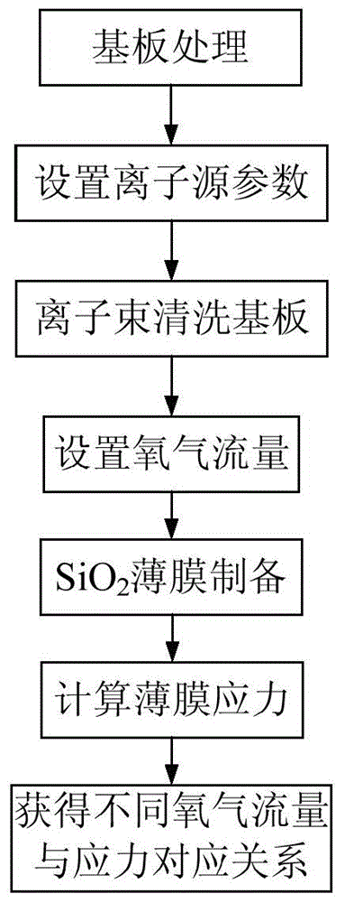
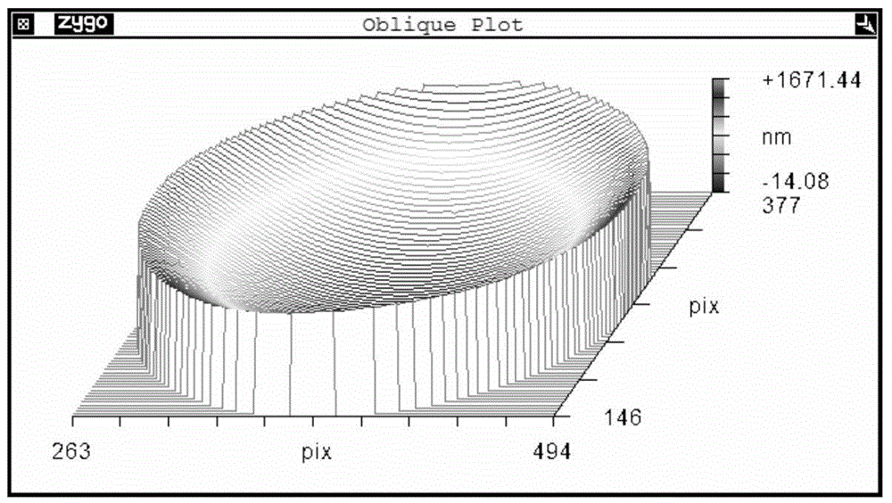
[0046] 1) Single-sided polished fused silica substrate (Φ25×1mm) is used for thin film stress test. Before coating, use the American ZYGO laser profiler to measure the surface shape of the substrate. The sample with the local error of surface shape ΔN2 For thin film deposition experiments, see image 3 ;
[0047] 2) Before coating, the substrate is chemically treated (chemical reagents include hydrochloric acid, ammonia water, hydrogen peroxide and deionized water), and then cleaned by ultrasonic waves. After the treatment is completed, dry it with a centrifugal dryer (ultrasonic frequency 3000kHz, ultrasonic time 15min ), after the treatment is completed, dry (6000r / min) with a centrifugal dryer;
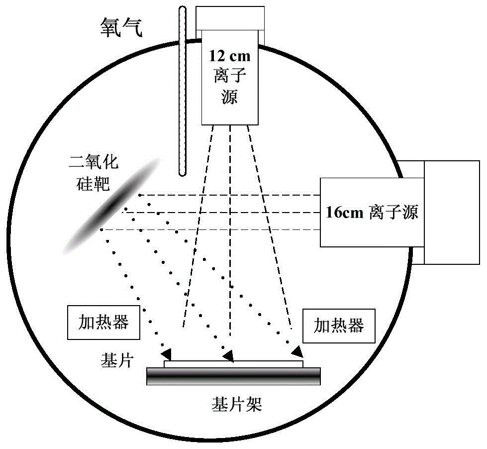
[0048] 3) The 16cm ion source is used as the sputtering ion source, the radio frequency frequency of the ion source is 13.56MHz, the ion beam voltage of the 16cm ion source is selected as 1250V, and the ion beam current is selected as 650mA;
[0049] 4) The target material is a hi...
Embodiment 2
[0053] 1) Single-sided polished fused silica substrate (Φ25×1mm) is used for thin film stress test. Before coating, use the American ZYGO laser profiler to measure the surface shape of the substrate. The sample with the local error of surface shape ΔN2 For thin film deposition experiments, see Figure 5 ;
[0054] 2) Before coating, the substrate is chemically treated (chemical reagents include hydrochloric acid, ammonia water, hydrogen peroxide and deionized water), and then cleaned by ultrasonic waves. After the treatment is completed, dry it with a centrifugal dryer (ultrasonic frequency 3000kHz, ultrasonic time 15min ), after the treatment is completed, dry (6000r / min) with a centrifugal dryer;
[0055] 3) The 16cm ion source is used as the sputtering ion source, the radio frequency frequency of the ion source is 13.56MHz, the ion beam voltage of the 16cm ion source is selected as 1250V, and the ion beam current is selected as 650mA;
[0056] 4) The target material is a h...
Embodiment 3
[0060] 1) Single-sided polished fused silica substrate (Φ25×1mm) is used for thin film stress test. Before coating, use the American ZYGO laser profiler to measure the surface shape of the substrate. The sample with the local error of surface shape ΔN2 For thin film deposition experiments, see Figure 7 ;
[0061] 2) Before coating, the substrate is chemically treated (chemical reagents include hydrochloric acid, ammonia water, hydrogen peroxide and deionized water), and then cleaned by ultrasonic waves. After the treatment is completed, dry it with a centrifugal dryer (ultrasonic frequency 3000kHz, ultrasonic time 15min ), after the treatment is completed, dry (6000r / min) with a centrifugal dryer;
[0062] 3) The 16cm ion source is used as the sputtering ion source, the radio frequency frequency of the ion source is 13.56MHz, the ion beam voltage of the 16cm ion source is selected as 1250V, and the ion beam current is selected as 650mA;
[0063] 4) The target material is a h...
PUM
| Property | Measurement | Unit |
|---|---|---|
| thickness | aaaaa | aaaaa |
| thickness | aaaaa | aaaaa |
| thickness | aaaaa | aaaaa |
Abstract
Description
Claims
Application Information