
A kind of method for preparing zno nano fence

A fence and nano technology, applied in the field of preparing ZnO nano-semiconductor materials, can solve problems such as complex technology

Active Publication Date: 2016-03-16
CHONGQING INST OF GREEN & INTELLIGENT TECH CHINESE ACADEMY OF SCI
View PDF2 Cites 0 Cited by
  • Summary
  • Abstract
  • Description
  • Claims
  • Application Information

AI Technical Summary

Problems solved by technology

This document uses a single layer of close-packed polystyrene microspheres (PS) instead of photoresist as a mask, and the technology is relatively complicated.

Method used


Image

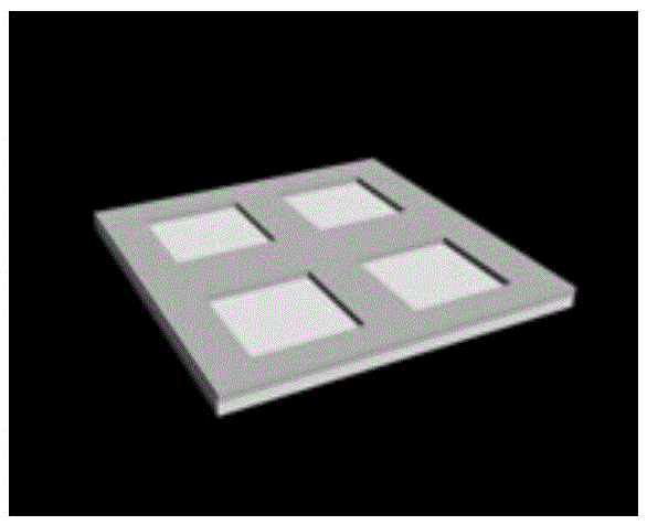
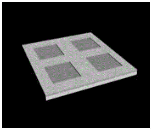
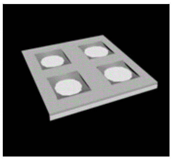
  • A kind of method for preparing zno nano fence
  • A kind of method for preparing zno nano fence
  • A kind of method for preparing zno nano fence

Examples


Embodiment 1

[0020] A certain pattern is photolithographically etched on the GaN substrate. The photolithography steps: firstly coat the photoresist (Su82000) film on the cleaned GaN substrate by spin coating method, then bake at 120°C for 20min, UV exposure (3mw, 30s) is used under the cover of the hole mask, the exposed part is washed away in the developer, and the substrate after photolithography is obtained by baking at 120°C for more than 20min. Then apply 5mM HAuCl 4 Mix the solution with 0.2v / v% EG, heat the substrate to 90°C, and wash off the photoresist with acetone after the solvent is completely volatilized; put the treated substrate into a vacuum tube furnace, and use a high-temperature chemical vapor deposition method (CVD), a boat filled with chemical reactants (zinc oxide powder and graphite powder) is placed in the middle of the high-temperature tube vacuum furnace, and the substrate is placed within 5 cm downstream of the air flow, and then the vacuum tube furnace is evacu...

Embodiment 2

[0022] A certain pattern is photolithographically etched on the GaN substrate. The photolithography steps: firstly coat the photoresist (Su82000) film on the cleaned GaN substrate by spin coating method, then bake at 120°C for 20min, UV exposure (3mw, 30s) is used under the cover of the hole mask, the exposed part is washed away in the developer, and the substrate after photolithography is obtained by baking at 120°C for more than 20min. Then apply 5mM HAuCl 4 Mix the solution with 0.2v / v% ethanol, heat the substrate to 100°C, and wash off the photoresist with acetone after the solvent is completely volatilized; put the treated substrate into a vacuum tube furnace, and use a high-temperature chemical vapor deposition method (CVD), place a boat filled with chemical reactants (zinc oxide powder and graphite powder) in the middle of the high-temperature tube-type vacuum furnace, place the substrate within 8cm of the downstream position of the airflow, and then use a mechanical pu...

Embodiment 3

[0024] A certain pattern is photolithographically etched on the GaN substrate. The photolithography steps: firstly coat the photoresist (Su82000) film on the cleaned GaN substrate by spin coating method, then bake at 120°C for 20min, UV exposure (3mw, 30s) is used under the cover of the hole mask, the exposed part is washed away in the developer, and the substrate after photolithography is obtained by baking at 120°C for more than 20min. Then apply 5mM HAuCl 4 Mix the solution with 0.2v / v% acetaldehyde, heat the substrate to 100°C, and wash off the photoresist with acetone after the solvent is completely volatilized; put the treated substrate into a vacuum tube furnace, and use high-temperature chemical vapor deposition Method (CVD), place a boat filled with chemical reactants (zinc oxide powder and graphite powder) in the middle of the high-temperature tube-type vacuum furnace, place the substrate within 8cm of the downstream position of the airflow, and then use a mechanical...


PUM


Abstract

The invention discloses a method for preparing a ZnO nano fence. The method is characterized by comprising the following steps: (1) a GaN substrate is photoetched; (2) the substrate is coated with gold catalyst reaction solution; (3) the substrate is heated and the solution is contracted; (4) gold is reduced from the solution and is in closed-loop distribution; and (5) a ZnO nanowire fence is grown in a catalyst-induced way by a CVD method. Gold nanoparticle distribution is controlled according to the hydrophobicity-hydrophilicity of the surface of the substrate after photoetching so as to inductively grow a nanowire fence. Unlike traditional control methods, the method of the invention has obvious innovative significance and a wider range of applications.

Description

technical field [0001] The invention relates to a method for preparing ZnO nano semiconductor material, in particular to a method for preparing ZnO nano barriers. Background technique [0002] As a semiconductor material with excellent piezoelectric and photoelectric properties, zinc oxide (ZnO) has excellent electrical, optical and chemical stability. Compared with semiconductor materials such as Si and GaN, it has a large band gap ( Eg=3.37eV) and high exciton binding energy (60meV), the one-dimensional ZnO nanostructure has a unique shape and excellent performance, and has been made into a variety of one-dimensional nanostructures, such as nanorods, nanowires, nanotubes , nanobelts, nanocombs, nanosprings, nanobows and nanothrusters are widely used in new nanodevices and systems such as nanogenerators, nanolasers, LEDs, sensors, and solar cells. Heterojunction semiconductor devices composed of third-generation semiconductor materials ZnO and GaN have shown great applicat...

Claims


Application Information

Patent Timeline
Patent Type & Authority Patents(China)
IPC IPC(8): H01L21/308C23C18/44C23C16/40C23C28/00B82Y40/00
CPCB82Y40/00C23C16/407C23C18/44C23C28/345H01L21/308
Inventor 王亮陆文强宋金会冯双龙王凤丽李振湖
Owner CHONGQING INST OF GREEN & INTELLIGENT TECH CHINESE ACADEMY OF SCI
Learn More