Thermopile infrared detector and manufacturing method thereof

A technology of an infrared detector and a manufacturing method, which can be applied to electric radiation detectors and other directions, can solve the problems of difficult control of lens curvature, chip distance, focus deviation, etc. The effect of matching and transmission complete suppression

Inactive Publication Date: 2015-04-22
HANGZHOU SILAN INTEGRATED CIRCUIT
View PDF4 Cites 31 Cited by
  • Summary
  • Abstract
  • Description
  • Claims
  • Application Information

AI Technical Summary

Problems solved by technology

However, the curvature of the lens and the distance from the chip are difficult to control, and it is easy to cause focus deviation

Method used


Image

  • Thermopile infrared detector and manufacturing method thereof
  • Thermopile infrared detector and manufacturing method thereof
  • Thermopile infrared detector and manufacturing method thereof

Examples


no. 1 example

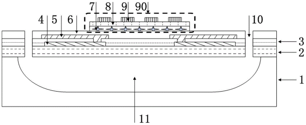
[0077] refer to figure 1 , the thermopile infrared detector can include: a substrate 1 with a cavity 11 in the substrate 1; a dielectric support film 2 positioned above the cavity 11 and supported by the substrate 1; a thermopile positioned as a dielectric above the cavity 11 on the supporting film 2; a passivation layer 6 covering the thermopile; a metamaterial structure 90 located on the passivation layer 6 above the thermopile. Wherein, the substrate 1 and the metamaterial structure 90 serve as the cold junction region and the hot junction region of the thermopile respectively.

[0078] Wherein, the substrate 1 may be various semiconductor substrates in a conventional CMOS process, such as a single crystal silicon wafer or an SOI silicon wafer.

[0079] The material of the dielectric support film 2 may be silicon oxide or silicon nitride, or the dielectric support film 2 may be a composite dielectric film formed of silicon oxide and silicon nitride.

[0080] Thermopiles c...

no. 2 example

[0106] refer to Figure 6 , Figure 6 The cross-sectional structure of the thermopile infrared detector of the second embodiment is shown, and its structure is basically the same as that of the first embodiment, except that the cavity 11 has an open opening on the back of the substrate 1 .

[0107] The manufacturing method of the thermopile infrared detector of the second embodiment is basically the same as that of the first embodiment, the difference lies in the formation method of the cavity 11 and the release method of the thermopile device. After the fabrication of the metamaterial structure is completed, the backside of the substrate 1 is etched and / or wet-etched to form a cavity 11 in the substrate 1 below the thermopile. After the cavity is formed, the dielectric support film 2 above the cavity 11 forms a suspended film structure, and the dielectric support film 2, thermopile and passivation layer 6 form a sandwich structure, thereby releasing the thermopile device. A...

no. 3 example

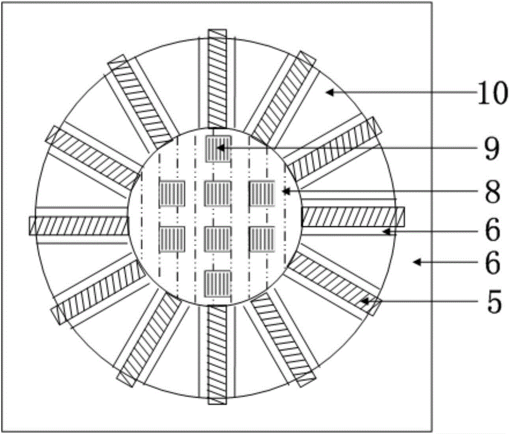
[0110] refer to Figure 7 , Figure 7 The cross-sectional structure of the thermopile infrared detector of the third embodiment is shown. As a preferred embodiment, in the direction perpendicular to the surface of the substrate 1, a plurality of intermediate dielectric layers 8 and a plurality of metal microstructure layers 9 are stacked, and a plurality of intermediate dielectric layers 8 and metal microstructure layers 9 spaced between each other. In other words, a plurality of intermediate dielectric layers 8 and a plurality of metal microstructure layers 9 are sequentially cascaded in a vertical direction in a manner of being spaced apart from each other. For example, Figure 7 It contains three intermediate dielectric layers 8 and three metal microstructure layers 9 .

[0111] Wherein, each intermediate dielectric layer 8 may be made of different dielectric materials, or may be the same dielectric material with different thicknesses. Metal microstructure layers 9 of ...


PUM


Abstract

The invention provides a thermopile infrared detector and a manufacturing method of the thermopile infrared detector. The thermopile infrared detector comprises a substrate, a dielectric supporting film, a thermopile, a metamaterial structure, a middle dielectric layer and a metal micro structure layer, wherein a cavity is formed in the substrate, the dielectric supporting film is located above the cavity and supported by the substrate, the thermopile is located on the dielectric supporting film above the cavity, the metamaterial structure is located above the thermopile and comprises a metal plane reflecting mirror, the middle dielectric layer is located on the metal plane reflecting mirror, the metal micro structure layer is located on the middle dielectric layer and comprises one or more structural period units, and each structural period unit comprises one or more geometric figure units having the light adsorption enhance effect within the infrared spectrum range. Due to the thermopile infrared detector, perform absorption within the infrared band broad spectrum range can be achieved, the infrared adsorption rate and the responding rate of the thermopile infrared detector can be improved, and the manufacturing method is compatible with a conventional CMOS technology.

Description

technical field [0001] The invention relates to thermopile infrared detector technology, in particular to a thermopile infrared detector which uses a metamaterial structure as an infrared absorber to enhance light absorption and a manufacturing method thereof. Background technique [0002] The thermopile infrared detector is one of the earliest researched and practical infrared imaging devices. As an uncooled infrared detector, it has the advantages of small size, light weight, no refrigeration, and high sensitivity. It is widely used in security monitoring , medical treatment, life detection and consumer products are widely used, and its development is more rapid. [0003] The working principle of the thermopile detector is mainly based on the Seebeck effect: two different materials or objects A and B with the same material but different work functions are connected at the hot junction, if there is a temperature difference ΔT between the hot junction and the cold zone, then...

Claims


Application Information

Patent Timeline
Patent Type & Authority Applications(China)
IPC IPC(8): G01J5/12
Inventor 孙福河闻永祥刘琛季锋陈雪平
Owner HANGZHOU SILAN INTEGRATED CIRCUIT
Why Eureka
Try Eureka