High-speed CMOS monolithic integration light receiver front end of cross coupling structure

A cross-coupling and monolithic integration technology, applied in the direction of electromagnetic receivers, can solve problems such as bandwidth and noise compromise, sacrifice circuit noise performance, sacrifice bandwidth, etc., to increase equivalent transconductance, suppress Bandwidth reduction, the effect of reducing input impedance

Inactive Publication Date: 2015-04-22
TIANJIN UNIV
View PDF10 Cites 17 Cited by
  • Summary
  • Abstract
  • Description
  • Claims
  • Application Information

AI Technical Summary

Problems solved by technology

The way to reduce the input impedance is usually achieved by adjusting the transistor size of the input point or introducing a feedback structure, but this is at the expense of circuit noise performance
Low noise front-end circuits are often impleme...

Method used


Image

  • High-speed CMOS monolithic integration light receiver front end of cross coupling structure
  • High-speed CMOS monolithic integration light receiver front end of cross coupling structure
  • High-speed CMOS monolithic integration light receiver front end of cross coupling structure

Examples


Embodiment Construction

[0031] In order to make the purpose, technical solution and advantages of the present invention clearer, the implementation manners of the present invention will be further described in detail below.

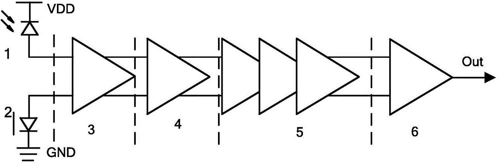
[0032] see figure 1 , the high-speed CMOS monolithic integrated optical receiver front-end circuit of the cross-coupling structure that the present invention proposes comprises:

[0033] Two photodetectors with completely symmetrical structures, among them, the first photodetector 1 converts the weak optical signal input by the optical fiber into an electrical pulse signal, and the second photodetector 2 is used to maintain the load balance of the differential input circuit and increase the reception machine bandwidth;

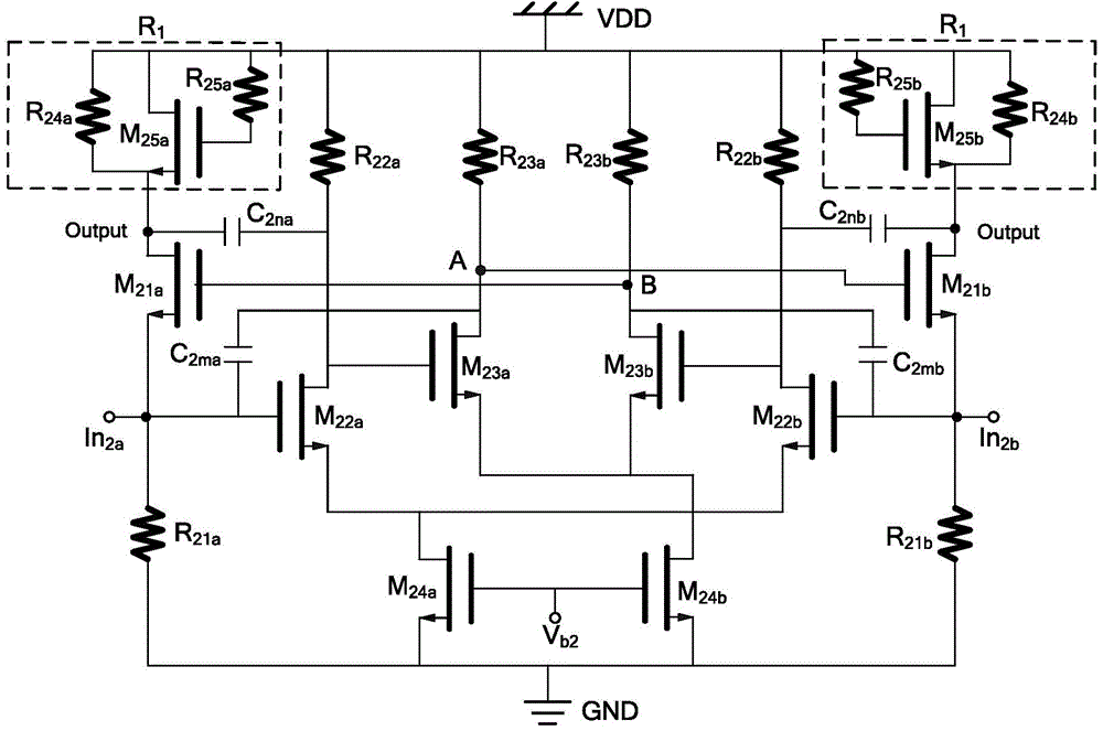
[0034] A transimpedance amplifier 3 of a differential cross-coupling structure, its function is to convert the current signal output by the photodetector (the first photodetector 1 and the second photodetector 2) into a voltage signal, and perform preliminary a...


PUM


Abstract

The invention discloses a high-speed CMOS monolithic integration light receiver front end of a cross coupling structure. The high-speed CMOS monolithic integration light receiver front end comprises a photoelectric detector of a completely-symmetric structure, a trans-impedance amplifier of a difference structure, a direct current excursion eliminating unit, a three-stage sequence cascaded difference limiting amplifier and an output buffer stage; the trans-impedance amplifier of the difference structure is used for converting current signals output by the photoelectric detector into voltage signals and conducting preliminary amplification; the direct current excursion eliminating unit is used for eliminating direct current excursion led in by non-balanced signals at the input end of the trans-impedance amplifier and enables common mode levels at the output end of the trans-impedance amplifier to be coincident; the three-stage sequence cascaded difference limiting amplifier is used for amplifying the voltage signals output by the trans-impedance amplifier to be at the voltage level needed by a digital processing unit. Through the adoption of the cross coupling structure, the noise in-phase counteraction technology and the parallel type active inductor design, a high-speed and high-sensitivity standard CMOS monolithic integration light receiver can be achieved.

Description

technical field [0001] The invention relates to the field of optical fiber communication system and optical interconnection, in particular to a high-speed CMOS single-chip integrated optical receiver front-end circuit with a cross-coupling structure. Background technique [0002] With the continuous development of communication and multimedia technology, people's demand for data information continues to increase. Because optical fiber communication has the advantages of high speed and large capacity, it is widely used in trunk network. However, for user terminals, limited by the cost of optoelectronic integrated chips, it is difficult to continue to advance the "last mile" of fiber-to-the-home. Therefore, the development of low-cost, high-performance optoelectronic integrated chips has become a research hotspot in the field of integrated optoelectronics. [0003] A fiber optic communication system usually consists of three parts: an optical transmitter, an optical fiber ch...

Claims


Application Information

Patent Timeline
IPC IPC(8): H04B10/69
Inventor 谢生陶希子毛陆虹高谦
Owner TIANJIN UNIV
Why Eureka
Try Eureka