Thallium-doped cesium iodide composite film and preparation method thereof

A composite film, cesium iodide technology, applied in vacuum evaporation plating, coating, sputtering plating and other directions, can solve the problems of high production cost, limited luminous intensity, limitations, etc., and achieve the effect of strong blue light emission characteristics

Inactive Publication Date: 2015-04-29
SHANGHAI INST OF CERAMIC CHEM & TECH CHINESE ACAD OF SCI
View PDF5 Cites 14 Cited by
  • Summary
  • Abstract
  • Description
  • Claims
  • Application Information

AI Technical Summary

Problems solved by technology

[0002] As we all know, thallium-doped cesium iodide (CsI:Tl) thin film material has been widely used as a scintillation thin film material in the fields of high energy physics, X-ray imaging screen and photocathode because of its good luminescent properties. However, often Requires thickness up to hundreds of microns, higher cost
The thinner (on the order of hundreds of nanometers) CsI:Tl film material in the prior art has limited luminous intensity, which limits its application in many fields, such as the field that requires blue light
At the same time, due to the high production cost of gallium nitride materials that can emit blue light, researchers have begun to look for new materials to replace it.

Method used


Image

  • Thallium-doped cesium iodide composite film and preparation method thereof
  • Thallium-doped cesium iodide composite film and preparation method thereof
  • Thallium-doped cesium iodide composite film and preparation method thereof

Examples


Embodiment 1

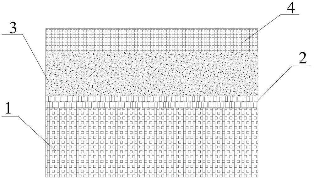
[0022] 1. Rinse the silicon sheet twice with pure water, then ultrasonically clean it in alcohol for 10 minutes, take it out and dry it naturally for later use;

[0023] 2. Use a copper plate as the target material, and deposit a copper film layer with a thickness of 10nm on the Si sheet at a rate of 0.02-0.5nm / s by ion beam sputtering;

[0024] Three, use commercially available CsI:Tl single crystal again as target material, deposit the CsI:Tl film layer that thickness is 300nm on the copper thin film layer surface with the method for ion beam sputtering;

[0025] 4. Finally use SiO 2 As the target material, a moisture-proof protective film with a thickness of 50nm was deposited on the surface of the CsI:Tl film layer by ion beam sputtering.

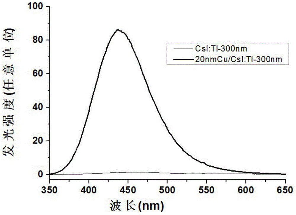
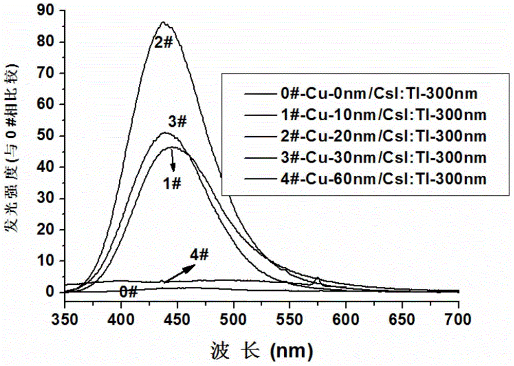
[0026] The sample prepared in this embodiment is marked as 1#, and its luminous properties are as follows: image 3 shown.

Embodiment 2

[0030] 1. Rinse the Si sheet twice with pure water, then ultrasonically clean it in acetone for 10 minutes, take it out and dry it naturally for later use;

[0031] 2. Use a copper plate as the target material, and deposit a copper film layer with a thickness of 20nm on the Si sheet at a rate of 0.02-0.5nm / s by ion beam sputtering;

[0032] Three, use commercially available CsI:Tl single crystal again as target material, deposit the CsI:Tl film layer that thickness is 300nm on the copper thin film layer surface with the method for ion beam sputtering;

[0033] 4. Finally use SiO 2 The ceramic target is used as the target material, and a moisture-proof protective film with a thickness of 50nm is deposited on the surface of the CsI:Tl film layer by ion beam sputtering.

[0034] The sample prepared in this embodiment is marked as 2#, and its luminous properties are as follows: image 3 shown.

Embodiment 3

[0036] 1. Rinse the quartz sheet twice with pure water, then ultrasonically clean it in acetone for 10 minutes, take it out and dry it naturally for later use;

[0037] 2. Use a copper plate as the target material, and deposit a copper film layer with a thickness of 30nm on the quartz plate at a rate of 0.02-0.5nm / s by ion beam sputtering;

[0038] Three, use commercially available CsI:Tl single crystal again as target material, deposit the CsI:Tl film layer that thickness is 300nm on the copper thin film layer surface with the method for ion beam sputtering;

[0039] 4. Finally use SiO 2 The ceramic target is used as the target material, and a moisture-proof protective film with a thickness of 50nm is deposited on the surface of the CsI:Tl film layer by ion beam sputtering.

[0040] The sample prepared in this embodiment is marked as 3#, and its luminous properties are as follows: image 3 shown.


PUM

PropertyMeasurementUnit
thicknessaaaaaaaaaa
thicknessaaaaaaaaaa
thicknessaaaaaaaaaa

Abstract

The invention discloses thallium-doped cesium iodide composite film and a preparation method thereof. The composite film is formed by sequentially coating a copper film layer, a thallium-doped cesium iodide film layer and a moistureproof protecting film layer on a base material from the upper part to the lower part; the preparation of the composite film can adopt the existing film coating technology to sequentially coating the copper film layer, the thallium-doped cesium iodide film layer and the moisture protecting film layer on the base material. Research shows that the composite film has the advantages that as a metal Cu film and a CsI:Tl film have efficient metal plasma enhanced luminescence effect, compared with a film, without an added metal Cu film layer, the luminescent intensity of the composite film is furthest increased by more than 85 times in a 400 to 450 nm blue band, and the composite film has strong blue-light emitting feature, and is expected to be applied to photoelectron fields, such as LED and the like.

Description

technical field [0001] The invention relates to a thallium-doped cesium iodide composite thin film and a preparation method thereof, belonging to the technical field of luminescent materials. Background technique [0002] As we all know, thallium-doped cesium iodide (CsI:Tl) thin film materials have been widely used as scintillation thin film materials in the fields of high-energy physics, X-ray imaging screens, and photocathodes because of their good luminescent properties. However, often Thicknesses up to several hundred microns are required, and the cost is high. The thinner (on the order of hundreds of nanometers) CsI:Tl film material in the prior art has limited luminous intensity, which limits its application in many fields, such as the field that requires blue light. At the same time, due to the high production cost of gallium nitride materials that can emit blue light, researchers have begun to look for new materials to replace it. Contents of the invention [00...

Claims


Application Information

Patent Timeline
Patent Type & Authority Applications(China)
IPC IPC(8): C23C14/16C23C14/10C23C14/46
CPCC23C14/16C23C14/0694C23C14/10C23C14/46
Inventor 刘光辉刘茜周真真费凡魏钦华杨华
Owner SHANGHAI INST OF CERAMIC CHEM & TECH CHINESE ACAD OF SCI
Why Eureka
Try Eureka