Fabrication method of rfldmos device

A manufacturing method and device technology, applied in the fields of semiconductor/solid-state device manufacturing, semiconductor devices, electrical components, etc., can solve the problems of consuming process steps, high manufacturing cost, multiple process steps, etc., so as to reduce process costs and improve gate reliability. , the effect of simple production process

Active Publication Date: 2017-08-08
SHANGHAI HUAHONG GRACE SEMICON MFG CORP
View PDF6 Cites 0 Cited by
  • Summary
  • Abstract
  • Description
  • Claims
  • Application Information

AI Technical Summary

Problems solved by technology

Both methods consume a large number of process steps
[0004] In the prior art, the formation of the thick field oxide layer and the formation of the pad oxide layer under the fishbone grid are both carried out separately, and each requires more process steps, so the process is complicated and the production cost is high.

Method used


Image

  • Fabrication method of rfldmos device
  • Fabrication method of rfldmos device
  • Fabrication method of rfldmos device

Examples


Embodiment Construction

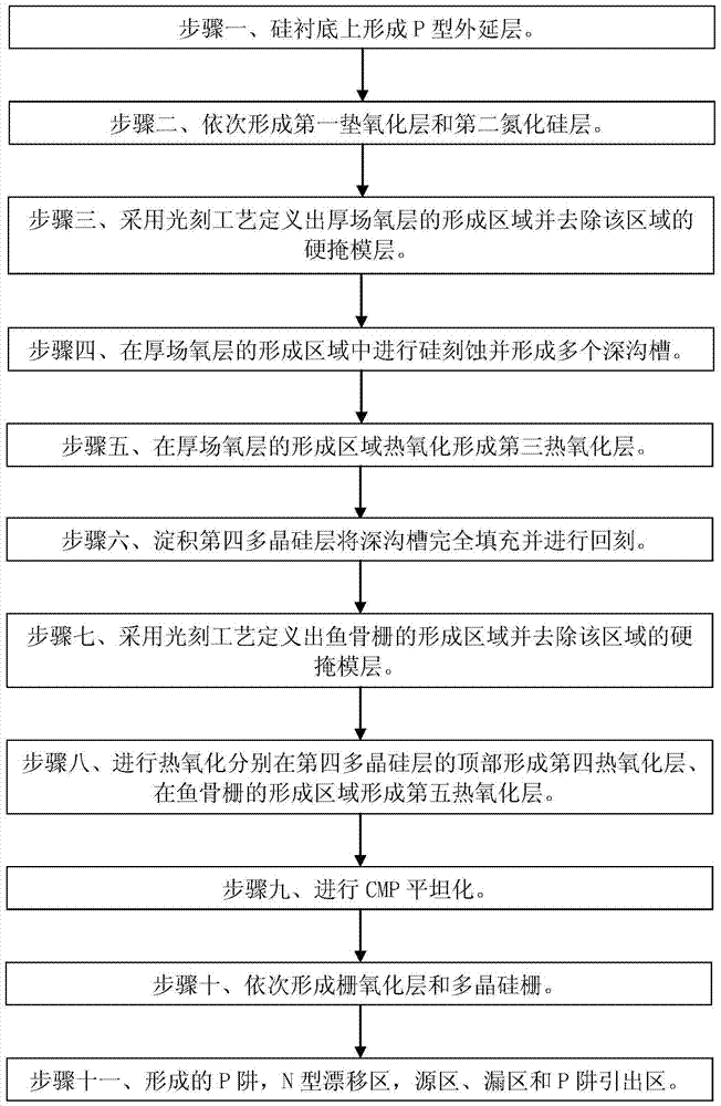
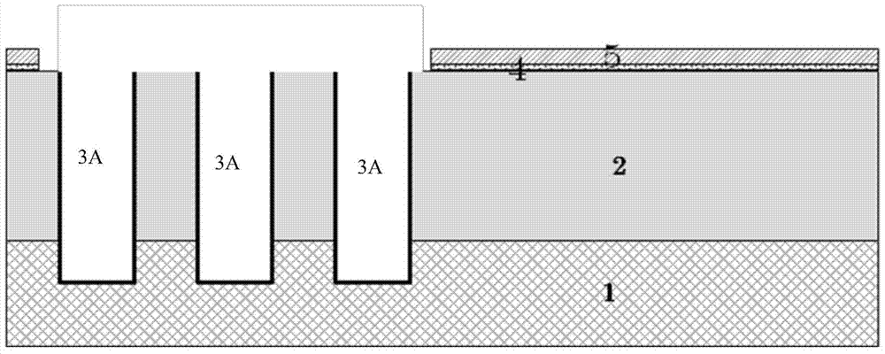
[0031] like figure 1 Shown is the flow chart of the method of the embodiment of the present invention; Figure 2 to Figure 8 Shown is a schematic diagram of the device structure in each step of the method of the embodiment of the present invention. The manufacturing method of the RFLDMOS device of the embodiment of the present invention comprises the following steps:

[0032] Step 1, such as figure 2 As shown, a lightly doped P-type epitaxial layer 2 is formed on a P-type heavily doped silicon substrate 1 . Preferably, the thickness of the P-type epitaxial layer 2 is 5 microns to 10 microns.

[0033] Step two, such as figure 2 As shown, the first pad oxide layer 4 and the second silicon nitride layer 5 are sequentially formed on the P-type epitaxial layer 2, and the first pad oxide layer 4 and the second silicon nitride layer 5 are composed of hard mask layer. Preferably, the thickness of the first pad oxide layer 4 is The thickness of the second silicon nitride laye...


PUM

PropertyMeasurementUnit
thicknessaaaaaaaaaa
thicknessaaaaaaaaaa
thicknessaaaaaaaaaa

Abstract

The invention discloses a manufacturing method of an RFLDMOS (radio frequency laterally diffused metal oxide semiconductor) device. The manufacturing method comprises steps as follows: a P-type epitaxial layer is formed on a silicon substrate; a first liner oxide layer and a second silicon nitride layer are sequentially formed; a forming region of a thick field oxide layer is defined, and a hard mask layer in the region is removed; multiple deep grooves are formed in the forming region of the thick field oxide layer; third thermal oxidation layers are formed in the forming region of the thick field oxide layer; fourth polycrystalline silicon layers are deposited, the deep grooves are completely filled with the fourth polycrystalline silicon layers, and an etch-back process is performed; a forming region of a fishbone gate is defined, and a hard mask layer in the region is removed; thermal oxidation is performed, fourth thermal oxidation layers are formed at the tops of the fourth polycrystalline silicon layers and a fifth thermal oxidation layer is formed in the forming region of the fishbone region; CMP (chemical mechanical polishing) flattening is performed; a gate oxide layer and a polysilicon gate are sequentially formed; a P well, an N-type drift region, a source region, a drain region and a P-well extraction region are formed. The manufacturing method enables a manufacturing process of the liner oxide layer under the fishbone gate to be simple and reduces the process cost.

Description

technical field [0001] The invention relates to a semiconductor integrated circuit manufacturing process method, in particular to a radio frequency lateral diffusion metal oxide semiconductor (RFLDMOS) device manufacturing method. Background technique [0002] In the existing RFLDMOS process flow, in order to improve the output capacitance of RFLDMOS devices and improve the RF performance of the device, it is often necessary to use a thick field oxide layer (G-Field) process as deep as 10 microns to reduce the device output capacitance. The thick field oxide layer is formed Right below the drain pad, when the thickness of the thick field oxygen layer increases, the thickness of the dielectric layer between the drain and the substrate increases, so the parasitic capacitance formed between the drain and the substrate will decrease, so by increasing The thickness of the thick field oxide layer can reduce the output capacitance of the device. Since the thick-field oxygen layer ...

Claims


Application Information

Patent Timeline
Patent Type & Authority Patents(China)
IPC IPC(8): H01L21/336H01L21/28
CPCH01L21/28158H01L29/7816H01L29/7825
Inventor 遇寒李昊周正良
Owner SHANGHAI HUAHONG GRACE SEMICON MFG CORP
Why Eureka
Try Eureka