
Preparation method of hybridized hierarchical structure sensitive thin-film sensing device based on two-dimensional material
A sensing device and a hierarchical structure technology, applied in the field of gas sensors and sensitive electronics, can solve the problem of inability to detect low concentration of acetone gas, and achieve the effects of good gas sensing characteristics, good uniformity and simple preparation method
- Summary
- Abstract
- Description
- Claims
- Application Information
AI Technical Summary
Problems solved by technology
Method used
Image

Examples
preparation example Construction
[0019] The preparation method of the above-mentioned hybrid hierarchical structure sensitive thin-film sensor device based on two-dimensional materials proposed by the present invention, the process flow includes the following steps:
[0020] 1) Preparation of interdigitated electrode device:
[0021] 1.1) Cleaning the single crystal semiconductor substrate 1: Put the single crystal semiconductor substrate into a mixture of hydrogen peroxide and concentrated sulfuric acid with a volume ratio of 1:4 and cook at 80-85°C for 10-15 minutes to remove surface stains and use deionized Rinse with water for 10-15 minutes, dry for later use; wherein, the single-crystal semiconductor substrate is an N-type phosphorus-doped single-polish silicon substrate, (100) crystal orientation, and a resistivity of 1-10Ω·cm;
[0022] 1.2) Growing insulating layer 2: growing silicon dioxide (SiO2) by thermal oxidation 2 ), the thickness is 100-300nm, after the oxidation is completed, the SiO 2 Prote...
Embodiment 1
[0044] Embodiment 1 is a typical example of the content of the present invention.
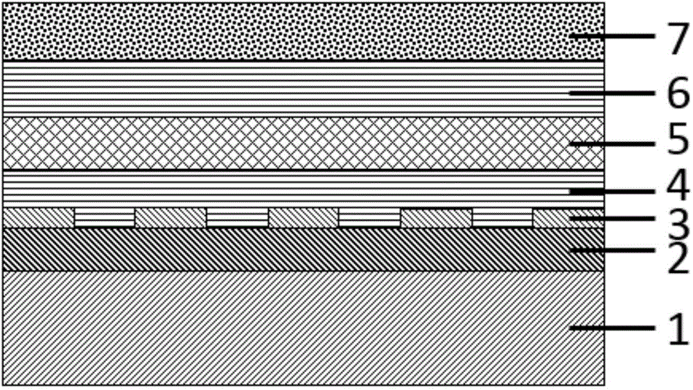
[0045] The hybrid hierarchical structure sensitive thin film sensing device based on two-dimensional materials in this embodiment, such as figure 1 As shown, it includes a single crystal semiconductor substrate 1, an insulating layer 2, an interdigital electrode 3, a first PDDA thin film layer 4, a reduced graphene oxide thin film layer 5, a second PDDA thin film layer 6, and a ZnO-PSS thin film 7. Among them, the single crystal semiconductor substrate 1 used is N-type single-polished Si, (100) crystal orientation, resistivity 3-6Ω·cm, and thickness 470um; the insulating layer 2 is SiO grown by thermal oxidation. 2 layer with a thickness of 1000nm; electrode 3 is a Ti / Au laminated interdigitated structure with a thickness of 10 / 80nm; film layer 4 is a PDDA film deposited by self-assembly method; film layer 5 is graphite oxide deposited by self-assembly method The graphene oxide film layer is o...
Embodiment 2
[0071] Embodiment 2 is a typical example of the content of the present invention.
[0072] The graphene-based hybrid hierarchical structure sensitive thin film sensor structure of this embodiment includes a single crystal semiconductor substrate 1, an insulating layer 2, an interdigital electrode layer 3, a first PDDA thin film layer 4, a reduced graphene oxide thin film layer 5, The second PDDA thin film layer 6, ZnO-PSS thin film 7. Among them, the single crystal semiconductor substrate 1 used is N-type single-polished Si, (100) crystal orientation, resistivity 3-6Ω·cm, and thickness 470um; the insulating layer 2 is SiO grown by thermal oxidation 2 layer with a thickness of 300nm; the electrode layer 3 is a Ti / Au laminated interdigitated structure with a thickness of 30 / 120nm; the film layer 4 is a PDDA film deposited by a self-assembly method; the film layer 5 is an oxide film deposited by a self-assembly method. Graphene thin film layer, and obtained reduced graphene oxid...
PUM
| Property | Measurement | Unit |
|---|---|---|
| thickness | aaaaa | aaaaa |
| thickness | aaaaa | aaaaa |
| concentration | aaaaa | aaaaa |
Abstract
Description
Claims
Application Information