SiC metal oxide semiconductor (MOS) capacitor of Al2O3/LaScO3/SiO2 stacked gate dielectric layer and production method of SiC MOS capacitor

A gate dielectric layer and stacking technology, which is applied in semiconductor/solid-state device manufacturing, circuits, electrical components, etc., can solve the problem that the thickness of SiO2 cannot be grown too thick, the interface state density between the dielectric and the SiC substrate is large, and the traps in the oxide layer Density and leakage current are large, to achieve the effect of increasing critical breakdown electric field, increasing channel mobility, reducing interface state density and boundary trap density

Inactive Publication Date: 2015-05-06
XIDIAN UNIV
View PDF3 Cites 0 Cited by
  • Summary
  • Abstract
  • Description
  • Claims
  • Application Information

AI Technical Summary

Problems solved by technology

However, SiO 2 / SiC MOS devices currently have the following disadvantages: First, compared with Si materials, the surface of SiC forms SiO through dry oxygen oxidation 2 The speed is quite slow, which increases the process cost, while SiO 2 The thickness of the can not grow too thick
Al currently 2 o 3 , HfO 2 , AlN and ZrO 2 There has been some research on high-k materials in SiC MOS, but high-k dielectrics directly replace SiO 2 The interface state density between the dielectric and the SiC substrate is larger, and the trap density and leakage current of the oxide layer are also larger

Method used


Image

  • SiC metal oxide semiconductor (MOS) capacitor of Al2O3/LaScO3/SiO2 stacked gate dielectric layer and production method of SiC MOS capacitor
  • SiC metal oxide semiconductor (MOS) capacitor of Al2O3/LaScO3/SiO2 stacked gate dielectric layer and production method of SiC MOS capacitor
  • SiC metal oxide semiconductor (MOS) capacitor of Al2O3/LaScO3/SiO2 stacked gate dielectric layer and production method of SiC MOS capacitor

Examples


Embodiment Construction

[0034] The technical solutions of the present invention will be described in further detail below with reference to the accompanying drawings and embodiments.

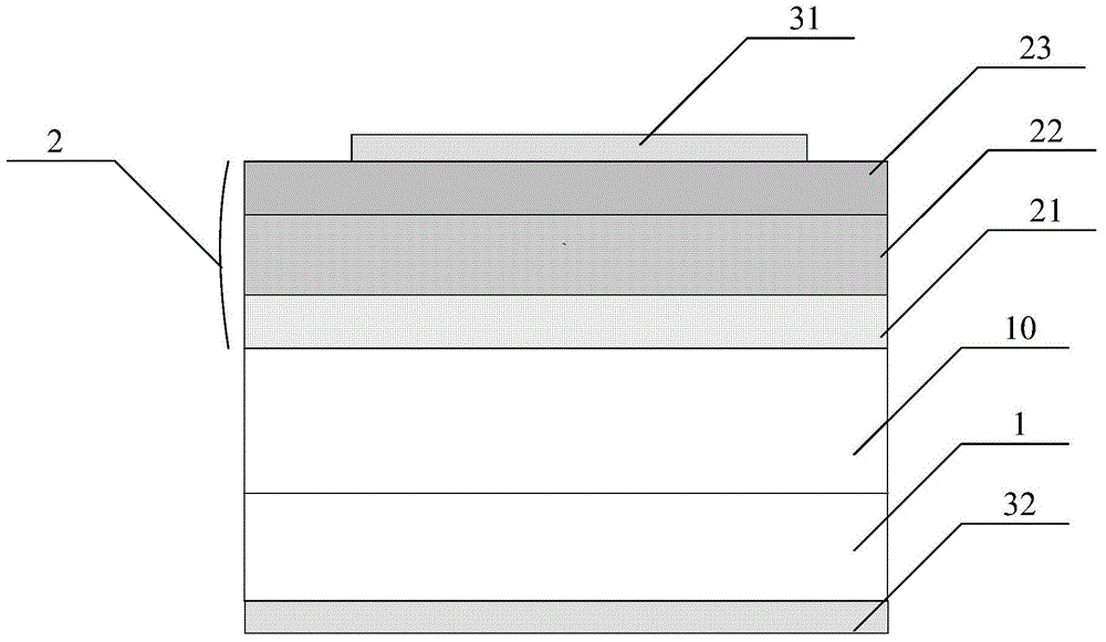
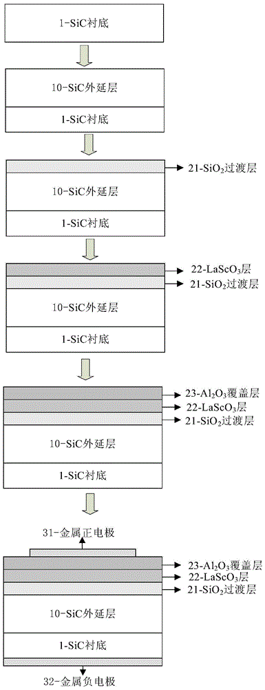
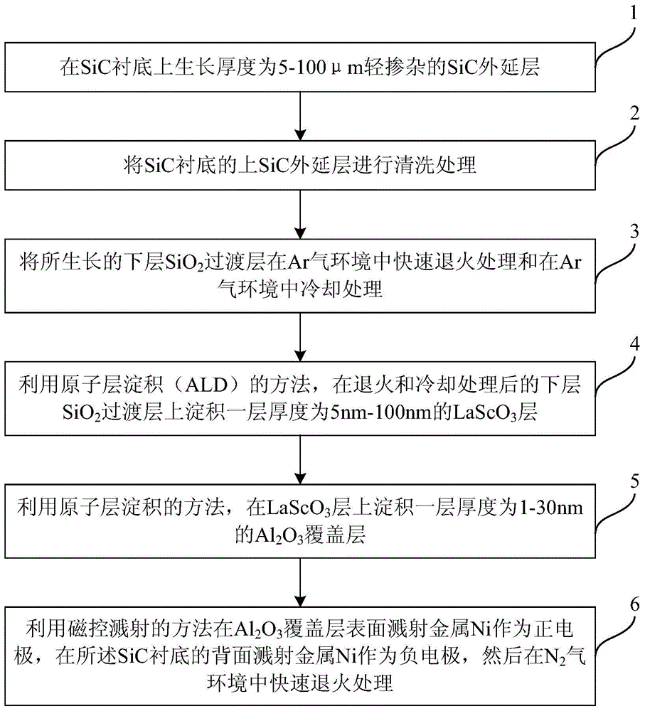
[0035] figure 1 For the present invention Al 2 o 3 / LaScO 3 / SiO 2 A schematic diagram of a SiC MOS capacitor with stacked gate dielectric layers, as shown in the figure, the present invention includes: SiC substrate 1 , SiC epitaxial layer 10 , stacked gate dielectric layer 2 and positive and negative electrodes 3 .

[0036] SiC epitaxial layer 10 is provided on SiC substrate 1;

[0037] The stacked gate dielectric layer 2 includes the lower SiO 2 Transition layer 21, LaScO 3 Layer 22 and Al 2 o 3 Covering layer 23; SiC epitaxial layer 10 is provided with lower layer SiO 2 Transition layer 21, lower layer SiO 2 The transition layer 21 is provided with LaScO 3 Layer 22, LaScO 3 Layer 22 is provided with Al 2 o 3 Overlay 23;

[0038] Positive electrode 31, negative electrode 32 and Al respectively 2 o 3...


PUM


Abstract

The invention relates to a SiC metal oxide semiconductor (MOS) capacitor of an Al2O3 / LaScO3 / SiO2 stacked gate dielectric layer and a production method of the SiC MOS capacitor. The SiC MOS capacitor comprises a heavily doped SiC substrate layer; a lightly doped SiC epitaxial layer is on the SiC substrate layer; the stacked gate dielectric layer comprises a lower SiO2 transition layer, a LaScO3 layer and an Al2O3 covering layer; the lower SiO2 transition layer is arranged on the SiC epitaxial layer; the LaScO3 layer is arranged on the lower SiO2 transition layer; the Al2O3 covering layer is arranged on the LaScO3 layer; and a positive electrode and a negative electrode are respectively connected with the surface of the Al2O3 covering layer and the back surface of the SiC substrate layer. By the SiC MOS capacitor of the stacked gate dielectric layer, the density of interface states and boundary traps is reduced, MOS channel mobility is improved, the gate leak current is reduced, voltage endurance capabitlity of the dielectric layer is improved, and the quality and the reliability of the SiC MOS capacitor are enhanced.

Description

technical field [0001] The invention relates to a SiC MOS capacitor and a manufacturing method thereof, in particular to an Al 2 o 3 / LaScO 3 / SiO 2 A SiC MOS capacitor with stacked gate dielectric layers and a manufacturing method thereof. Background technique [0002] With the continuous development of microelectronics technology and power electronics technology, practical applications have higher and higher performance requirements for devices working under conditions such as high temperature, high power, and high frequency. The first generation of semiconductor materials represented by Si and represented by GaAs The application of the second-generation semiconductor materials in these areas has become a bottleneck. Silicon carbide (SiC) material, as one of the typical representatives of the third-generation wide bandgap semiconductor materials, has a large bandgap, high critical breakdown electric field, high thermal conductivity, high electron saturation rate and hi...

Claims


Application Information

Patent Timeline
IPC IPC(8): H01L29/94H01L29/06H01L21/02C23C14/35
CPCH01L29/94C23C14/35H01L21/022H01L21/02293H01L29/408H01L29/42364
Inventor 贾仁需赵东辉吕红亮张玉明
Owner XIDIAN UNIV
Why Eureka
Try Eureka