A method for removing composite mask for high-energy ion implantation
A composite mask and high-energy ion technology, which is applied in the field of masks, can solve the problems of easy residual photoresist mask, many process errors in graphic size, and affecting the blocking effect of thin film masks, so as to avoid device process failure, Avoiding mask residues and shortening the deglue time
- Summary
- Abstract
- Description
- Claims
- Application Information
AI Technical Summary
Problems solved by technology
Method used
Image
Examples
Embodiment 1
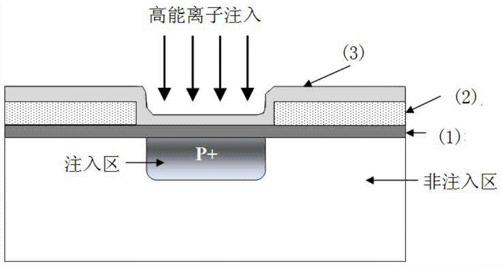
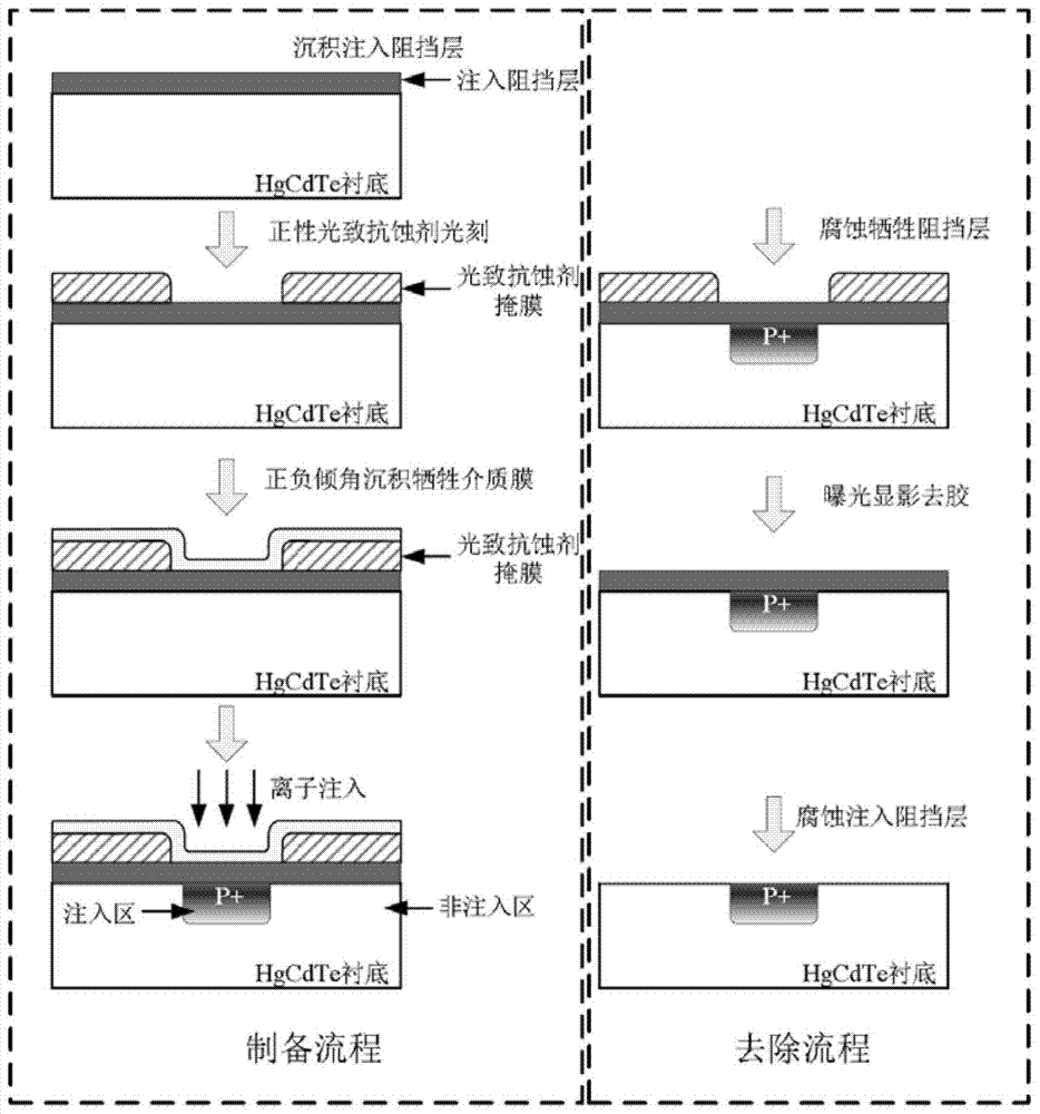
[0025] Using the mask preparation method described in the present invention, evaporation deposition, photolithography and positive and negative angle evaporation deposition are carried out on the surface of the HgCdTe epitaxial material chip. The preparation process is as follows figure 2 shown. First, a ~60nm thick cadmium telluride injection barrier layer was deposited by thermal evaporation on the surface of the HgCdTe epitaxial material chip after annealing treatment and surface corrosion treatment, the chip was cleaned, and a layer of thickness 2-3 microns was spin-coated on the chip surface. Thick positive photoresist, the chip is exposed to UV light with a photolithography plate, and after development and fixing, a photoresist injection mask is obtained.
[0026] Load the chip with the prepared mask pattern on the sample stage of the high vacuum thermal evaporation equipment, first rotate the sample stage at a 0° inclination angle, and deposit a ~20nm thick zinc sulfid...
Embodiment 2
[0030] Using the mask preparation method described in the present invention, evaporation deposition, photolithography and positive and negative angle sputtering deposition are carried out on the surface of the mercury cadmium telluride epitaxial material chip, and the preparation process is as follows figure 2shown. First, a ~20nm thick cadmium telluride injection barrier layer was deposited by thermal evaporation on the surface of the HgCdTe epitaxial material chip after annealing treatment and surface corrosion treatment, the chip was cleaned, and a layer of thickness 2-3 microns was spin-coated on the chip surface. Thick positive photoresist, the chip is exposed to UV light with a photolithography plate, and after development and fixing, a photoresist injection mask is obtained.
[0031] Load the chip with the mask pattern prepared on the sample stage of the magnetron sputtering equipment, first rotate the sample stage at a 0° inclination angle, and sputter a silicon dioxi...
Embodiment 3
[0035] Using the mask preparation method described in the present invention, evaporation deposition, photolithography and positive and negative angle evaporation deposition are carried out on the surface of the HgCdTe epitaxial material chip. The preparation process is as follows figure 2 shown. First, a cadmium telluride injection barrier layer with a thickness of 200 nm is deposited by thermal evaporation on the surface of the HgCdTe epitaxial material chip after annealing treatment and surface corrosion treatment, the chip is cleaned, and a layer of thickness 2-3 μm is spin-coated on the surface of the chip. Thick positive photoresist, the chip is exposed to UV light with a photolithography plate, and after development and fixing, a photoresist injection mask is obtained.
[0036] Load the chip with the prepared mask pattern on the sample stage of the high vacuum thermal evaporation equipment. First, rotate the sample stage at a 0° inclination angle to deposit a ~80nm thic...
PUM
 Abstract
Description
Claims
Application Information


