Driving method of gallium nitride transistor, driving circuit thereof, and fly-back converter using the circuit

A driving method and driving circuit technology, which are applied in the direction of high-efficiency power electronic conversion, adjustment of electrical variables, and output power conversion devices, can solve the problem of not reducing reverse conduction loss, etc. The effect of simple circuit structure

Inactive Publication Date: 2015-05-13
MORNSUN GUANGZHOU SCI & TECH +1
View PDF7 Cites 26 Cited by
  • Summary
  • Abstract
  • Description
  • Claims
  • Application Information

AI Technical Summary

Problems solved by technology

At present, for gallium nitride transistors used as control transistors in resonant converters or PWM soft switching converters working in the ZVS state, the industry has not yet reduced the reverse conduction loss caused by the dead time period introduced by the implementation of ZVS. program emerges

Method used


Image

  • Driving method of gallium nitride transistor, driving circuit thereof, and fly-back converter using the circuit
  • Driving method of gallium nitride transistor, driving circuit thereof, and fly-back converter using the circuit
  • Driving method of gallium nitride transistor, driving circuit thereof, and fly-back converter using the circuit

Examples


Embodiment 1

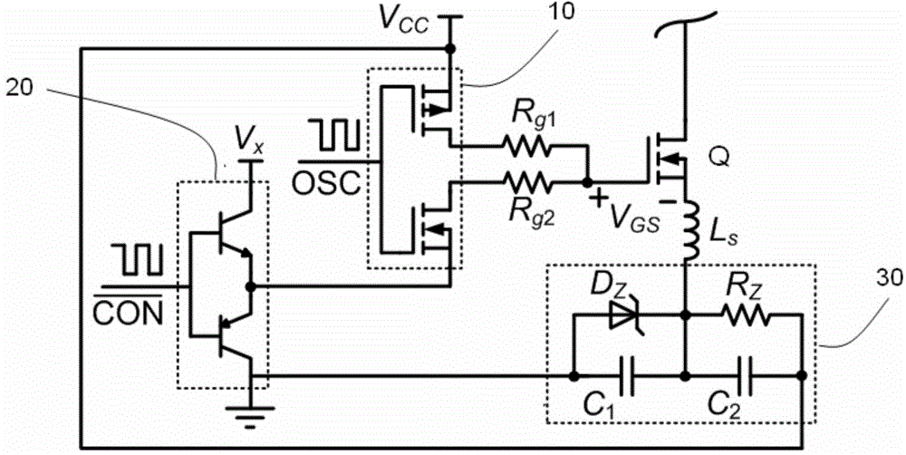
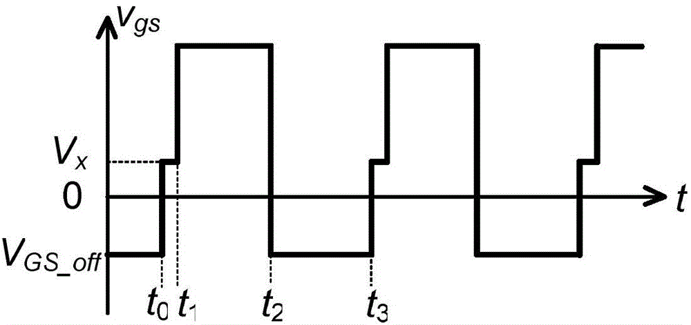
[0055] figure 1 The circuit diagram of the driving circuit of the gallium nitride transistor in the first embodiment of the present invention is given, wherein the inductance Ls represents the parasitic inductance in the circuit and the package, and this equivalent device is drawn for the convenience of explaining that the parasitic inductance will cause the turn-off time The oscillation problem of the driving voltage Vgs leads to the purpose of adding negative voltage to the driving.

[0056] A gallium nitride transistor driving circuit is composed of a switching tube Q, a driving pulse amplifying unit 10 , an intermediate level generating unit 20 and a negative voltage bias circuit 30 . Wherein, the switching tube Q is a gallium nitride transistor, the driving pulse amplifying unit 10 uses a single-channel low-side gate driver LM5114 of TI Company, and the intermediate level generating unit 20 is composed of an NPN triode and a PNP triode in the form of a totem pole. Negati...

Embodiment 2

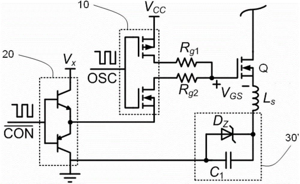
[0061] image 3 The driving circuit diagram of the gallium nitride transistor of the second embodiment of the present invention is given. The difference from the first embodiment is that the bias resistor R is omitted in the negative voltage bias circuit 30'. z and filter capacitor C 2 , using capacitance C 1 The charge stored in to ensure the Zener diode D z In Zener breakdown state, Zener diode D z The anode of the GaN transistor Q is connected to the source, and the Zener diode D z The cathode of the intermediate level generating unit is connected to the collector of the PNP transistor. The main advantage of this implementation is that two components are omitted and there is no longer a bias resistor R z on the loss. All the driving circuits using the gallium nitride transistor of the first embodiment in the following application examples can be replaced by the circuit of the embodiment.

Embodiment 3

[0063] Figure 4 It is the driving circuit diagram of the gallium nitride transistor of the third embodiment of the present invention. The difference from the second embodiment is that the connection position of the negative voltage bias circuit 30' has changed, and the source of the gallium nitride transistor and the Between the ground and the gate of the gallium nitride transistor, the specific connection relationship is that the Zener diode D z of the cathode and drive resistor R g1 connection, the Zener diode D z The anode of the GaN transistor Q is connected to the gate of the gallium nitride transistor Q. Compared with the previous two implementations, the advantage of this implementation is that the common ground of the driving circuit and the main circuit is realized. Similarly, all the driving circuits using the gallium nitride transistor of the first embodiment in the following application examples can be replaced by the circuits of the embodiment.

[0064] Figu...


PUM


Abstract

The invention discloses a driving method of a gallium nitride transistor and belongs to the field of DC-DC (direct current-direct current) power conversion. On one hand, a gallium nitride driving circuit is provided with a negative voltage driver based on a traditional gallium nitride driving chip, so that the gallium nitride transistor is accelerated in shutdown and the wrong conduction condition caused due to overlarge dv/dt on two electrodes of a drain source during shutdown is restrained. On the other hand, the driving method can solve the problem that after the gallium nitride transistor is disconnected, the reverse conduction loss is occurred when negative voltage is added into drive voltage; one intermediate level VM less than the starting voltage Vth is added in the reverse conduction time period so that the reverse conduction voltage is reduced from Vth + Vg _off to Vth - VM, and the reverse conduction loss is greatly reduced. The driving method can be applied to all occasions where the gallium nitride transistor is required for driving and especially used for driving the control tube of a resonant converter and the control tube of a PWM (Pulse-Width Modulation) soft switching converter.

Description

technical field [0001] The invention belongs to the technical field of power conversion, and in particular relates to a driving method and a circuit of a gallium nitride transistor of a DC-DC power converter and a flyback converter applying the circuit. Background technique [0002] With the rapid development of power electronics technology, power converters are developing towards high power density and high efficiency. The operating frequency of traditional power converters is generally tens of thousands to hundreds of kilohertz, and the dynamic response is slow. At the same time, the volume and weight of energy storage components (such as capacitors and inductors) are relatively large, which greatly reduces the power of the converter. density. The increase in operating frequency can effectively speed up the dynamic response speed of the converter and the power density of the converter. Therefore, the high frequency and high power density of converters are the development...

Claims


Application Information

Patent Timeline
Patent Type & Authority Applications(China)
IPC IPC(8): H02M1/08H02M3/335
CPCH02M1/08H02M3/33523H02M1/0054Y02B70/10
Inventor 董舟周嫄张之梁任小永余凤兵
Owner MORNSUN GUANGZHOU SCI & TECH
Why Eureka
Try Eureka