Diamond-like thick film, preparation method of diamond-like thick film and work-piece
A diamond thick film and diamond-like film technology, applied in the field of materials, can solve problems such as peeling failure and reduced matching degree, and achieve the effects of reducing stress, strong bonding force, and avoiding deterioration of mechanical properties
- Summary
- Abstract
- Description
- Claims
- Application Information
AI Technical Summary
Problems solved by technology
Method used
Image
Examples
preparation example Construction
[0048] The present invention also provides a method for preparing a diamond-like thick film, comprising the following steps:
[0049] Deposit a bonding layer and a transition layer sequentially on the surface of the workpiece to be plated;
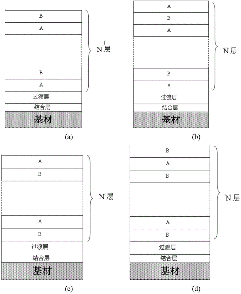
[0050] By changing the energy of carbon ions or carbon-hydrogen ion clusters, superimposed deposition of sp on the surface of the transition layer 3 Diamond-like subfilms with different bond contents, the sp 3 Diamond-like sub-films with different bond contents are stacked to form a diamond-like film layer compounded in the transition layer.
[0051] In the present invention, before depositing a diamond-like thick film on the surface of the workpiece to be plated, the surface of the workpiece to be plated needs to be pretreated, specifically:
[0052] (1) The workpiece to be plated is degreased with lye, rinsed with pure water, dehydrated and dried with hot air to remove rust, oil stains and other stains on the surface of the workpiece t...
Embodiment 1
[0097] Degrease the workpiece to be plated with a sodium hydroxide solution with a mass concentration of 1% to 3%, rinse with pure water, dehydrate and dry with hot air at 120°C to remove rust, oil stains and other stains on the workpiece; The plated workpiece is placed in the vacuum chamber, the vacuum chamber is evacuated, and the vacuum chamber is heated to 150°C at the same time. When the vacuum degree of the vacuum chamber is lower than 5×10 -4 After Pa, the vacuum chamber temperature was adjusted and stabilized at 120 °C.
[0098] Introduce argon gas into the vacuum chamber, run the anode layer ion source in the high-voltage low-current discharge mode to generate argon ions, and at the same time, turn on the bias power supply, where the bias power supply is a pulse power supply, and set the bias value to -1500V. The workpiece to be plated is cleaned by plasma glow for 45 minutes to obtain a clean workpiece to be plated.
Embodiment 2
[0100] Adopt magnetron sputtering method to deposit a layer of titanium binding layer on the surface of the clean workpiece to be plated provided in embodiment 1, the thickness of this binding layer is 0.1 micron, and the bias power supply is set to-120V in the deposition process, and the bias power supply can be DC power supply;
[0101] Secondly, a titanium carbide transition layer is deposited on the surface of the bonding layer by magnetron sputtering to obtain a workpiece to be plated on which the bonding layer and the transition layer are deposited. Wherein, the thickness of the transition layer is 0.1 micron; the bias power is set to -60V during the deposition process, and the bias power is a pulse power.
PUM
| Property | Measurement | Unit |
|---|---|---|
| thickness | aaaaa | aaaaa |
| thickness | aaaaa | aaaaa |
| thickness | aaaaa | aaaaa |
Abstract
Description
Claims
Application Information
 - R&D
- Intellectual Property
- Life Sciences
- Materials
- Tech Scout
- Unparalleled Data Quality
- Higher Quality Content
- 60% Fewer Hallucinations
Browse by: Latest US Patents, China's latest patents, Technical Efficacy Thesaurus, Application Domain, Technology Topic, Popular Technical Reports.
© 2025 PatSnap. All rights reserved.Legal|Privacy policy|Modern Slavery Act Transparency Statement|Sitemap|About US| Contact US: help@patsnap.com

