
Micro super capacitor nano-device based on porous graphene-supported polyaniline heterostructure and manufacturing method thereof

A technology of porous graphene and supercapacitors, applied in the manufacture of hybrid/electric double layer capacitors, hybrid capacitor electrodes, etc., can solve the problems of small capacitance and low utilization of the surface area of ​​electrode materials, so as to increase the contact area and increase the capacity and energy density, the effect of increasing conduction

Inactive Publication Date: 2015-05-20
WUHAN UNIV OF TECH
View PDF2 Cites 35 Cited by
  • Summary
  • Abstract
  • Description
  • Claims
  • Application Information

AI Technical Summary

Problems solved by technology

However, only the microporous surface that can be in contact with the electrolyte in the electrode material can generate capacitance. The deficiency of the existing electric double layer capacitors and pseudocapacitors is that the main part of the porous electrode surface area is micropores. Due to the effect of the surface tension of the electrolyte solution, It makes it difficult for the electrolyte solution to enter the micropores of the porous electrode, resulting in a low utilization rate of the surface area of ​​the electrode material, and even a phenomenon that some carbon electrode materials have a large specific surface area, but the capacitance after being made into a capacitor is not large.

Method used


Image

  • Micro super capacitor nano-device based on porous graphene-supported polyaniline heterostructure and manufacturing method thereof
  • Micro super capacitor nano-device based on porous graphene-supported polyaniline heterostructure and manufacturing method thereof
  • Micro super capacitor nano-device based on porous graphene-supported polyaniline heterostructure and manufacturing method thereof

Examples


Embodiment 1

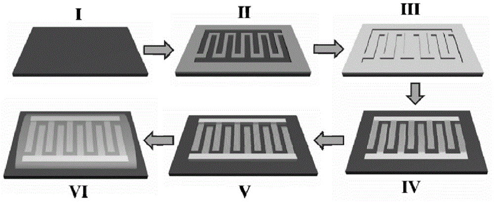
[0028] like figure 1 Shown, the preparation method of porous graphene supported polyaniline heterostructure base micro-supercapacitor nano-device, it comprises the following steps:

[0029] 1) Select the silicon substrate, cut the silicon substrate into an appropriate size, then ultrasonically clean the silicon substrate with isopropanol (IPA) for about 3 minutes, and dry it with nitrogen;

[0030] 2) Use a spin coater to spin coat a layer of 9000A on the substrate. The spin coating speed is 4000r / min, and the spin coating time is 40s.

[0031] 3) Etch the interdigitated electrode pattern on the spin-coated silicon wafer with a photolithography machine, and the exposure time is 28s;

[0032] 4) Development: soak the photoetched substrate in RD6 developer solution for 90s, then soak in deionized water for 30s, then soak in the second portion of deionized water for 30s, and blow dry with nitrogen;

[0033] 5) Metal Thermal Evaporation (PVD): Use a thermal evaporation coater to...

Embodiment 2

[0040] A method for preparing a porous graphene-supported polyaniline heterostructure-based miniature supercapacitor nano-device, comprising the steps of:

[0041] 1) Select the silicon substrate, cut the silicon substrate into an appropriate size, then ultrasonically clean the silicon substrate with isopropanol (IPA) for about 3 minutes, and dry it with nitrogen;

[0042] 2) Use a spin coater to spin coat a layer of 9000A on the substrate. The spin coating speed is 4000r / min, and the spin coating time is 40s.

[0043] 3) Etch the interdigitated electrode pattern on the spin-coated silicon wafer with a photolithography machine, and the exposure time is 28s;

[0044] 4) Development: soak the photoetched substrate in RD6 developer solution for 90s, then soak in deionized water for 30s, then soak in the second portion of deionized water for 30s, and blow dry with nitrogen;

[0045] 5) Metal Thermal Evaporation (PVD): Use a thermal evaporation coater to vapor-deposit metal to pre...

Embodiment 3

[0052] A method for preparing a porous graphene-supported polyaniline heterostructure-based miniature supercapacitor nano-device, comprising the steps of:

[0053] 1) Select polyethylene terephthalate, cut polyethylene terephthalate (PET) into an appropriate size, then ultrasonically clean PET with isopropyl alcohol (IPA) for about 3 minutes, and dry it with nitrogen ;

[0054] 2) Use a spin coater to spin coat a layer of 9000A on the PET substrate. The spin coating speed is 4000r / min, and the spin coating time is 40s.

[0055] 3) Use a photolithography machine to etch the interdigitated electrode pattern on the spin-coated PET substrate, and the exposure time is 28s;

[0056] 4) Development: soak the photoetched PET substrate in RD6 developer solution for 90s, then soak in deionized water for 30s, then soak in the second portion of deionized water for 30s, and blow dry with nitrogen;

[0057] 5) Metal Thermal Evaporation (PVD): Use a thermal evaporation coater to vapor-depo...


PUM

PropertyMeasurementUnit
Thicknessaaaaaaaaaa
Thicknessaaaaaaaaaa
Interdigital widthaaaaaaaaaa

Abstract

The invention relates to a micro super capacitor nano-device based on a porous-graphene-supported polyaniline heterostructure and a manufacturing method thereof. A symmetrical fork electrode structure is formed on a substrate material; forks are 100-200 nanometers in widths; the distances among the forks are 50-100 nanometers; electrolyte is added dropwise; in the fork electrode structure, gold serving as a current collector is taken as the first layer of an electrode material; porous graphene is attached to the gold and is taken as the second layer of the electrode material; polyaniline is coated on the porous graphene and is taken as the surface layer of the electrode material; the gold is 10-20 nanometers in thickness; the porous graphene is 20-40 nanometers in thickness; the polyaniline is 20-40 nanometers in thickness; the electrode material is 50-100 nanometers in total thickness. The micro super capacitor nano-device has the beneficial effects that a micro energy storing device can store more energy on the premise of ensuring high electronic conduction, so that the capacity and energy density of a super capacitor are further increased.

Description

technical field [0001] The invention relates to a porous graphene-supported polyaniline heterostructure-based micro-supercapacitor nano-device and a preparation method thereof. Background technique [0002] With the rapid growth of population and the rapid development of social economy, resources and energy are gradually depleted, and the ecological environment is deteriorating. In order to meet the needs of consumers and environmental protection requirements, people put forward the following requirements for power supply systems: excellent performance, Long life, low price, wide range of applications, etc. In addition, with the continuous advancement of human science and technology, the protection of the earth's environment has also received public attention. Therefore, human society is stepping up the development of new energy sources, and the new application fields of energy storage equipment are also expanding. [0003] Supercapacitor is a new type of energy storage dev...

Claims


Application Information

Patent Timeline
IPC IPC(8): H01G11/26H01G11/28H01G11/24H01G11/30H01G11/36H01G11/84H01G11/86
CPCY02E60/13H01G11/26H01G11/24H01G11/28H01G11/30H01G11/36H01G11/84H01G11/86
Inventor 麦立强肖蓓田晓聪许絮晏梦雨
Owner WUHAN UNIV OF TECH
Learn More