

Copper nanometer wire-based copper-copper bonding process
A technology of copper nanowires and copper-copper bonding, applied in semiconductor devices, electrical components, circuits, etc., can solve problems such as damage to devices, high thermal stress and thermal deformation, and achieve protection of devices, lower temperature and pressure, and controllability strong effect
- Summary
- Abstract
- Description
- Claims
- Application Information
AI Technical Summary
Problems solved by technology
Method used
Image

Examples
Embodiment 1
[0043] The copper-copper bonding process based on copper nanowires includes the following steps:
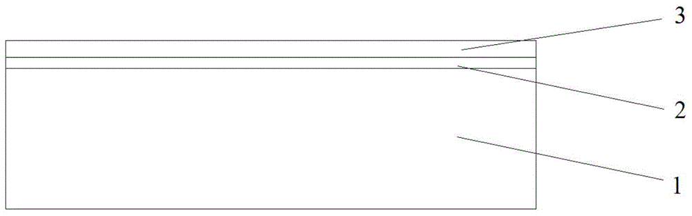
[0044] (1) Using magnetron sputtering to sequentially sputter a layer of adhesion layer Ti and seed layer Au on the clean wafer surface, the thicknesses are 20nm and 50nm respectively.
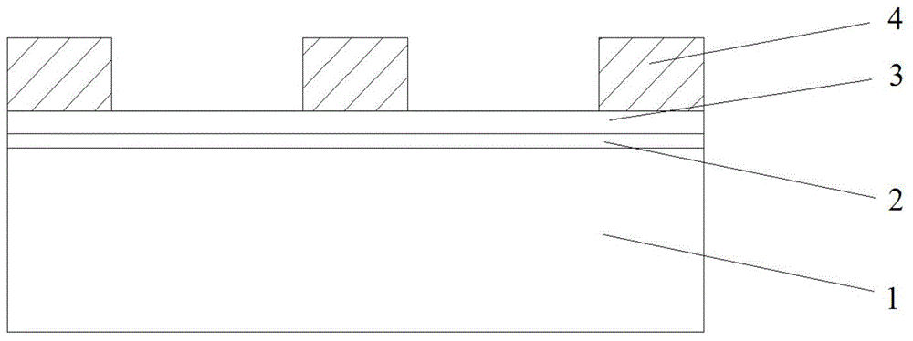
[0045] (2) Spin-coat PR1-4000A positive photoresist with a thickness of 5 μm on the surface of the seed layer, use a pattern mask containing an area-array circular hole, the circular hole area is transparent, the diameter of the circular hole is 5 μm, and the center distance of the circular hole 10 μm, use MA6 contact photolithography machine for photolithography, and use RD6 developer for development, rinse with deionized water and blow dry with nitrogen gun.
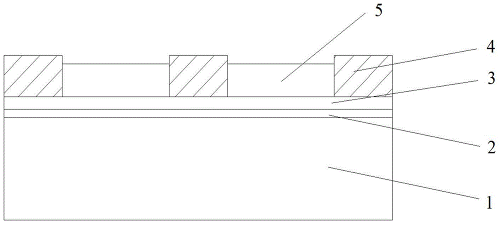
[0046] (3) Put the pattern obtained by photolithography into the copper plating solution for electroplating. The copper plating solution is SYSB2210 bump copper plating solution from Xinyang Company. The electroplating current density is ...
Embodiment 2
[0053] The copper-copper bonding process based on copper nanowires includes the following steps:
[0054] (1) Using magnetron sputtering to sequentially sputter a layer of adhesion layer TiW and seed layer Au on the clean wafer surface, the thicknesses are 50nm and 100nm respectively.
[0055] (2) Spin-coat PR1-12000A positive photoresist with a thickness of 20 μm on the surface of the seed layer, use a pattern mask containing an area-array circular hole, the circular hole area is transparent, the diameter of the circular hole is 20 μm, and the center distance of the circular hole 80 μm, use MA6 contact photolithography machine for photolithography, and use RD6 developer for development, rinse with deionized water and blow dry with nitrogen gun.
[0056] (3) Put the pattern obtained by photolithography into the copper plating solution for electroplating. The copper plating solution selects SYSB2210 bump copper plating solution from Xinyang Company, and the electroplating curre...
Embodiment 3
[0063] The copper-copper bonding process based on copper nanowires includes the following steps:
[0064] (1) Using magnetron sputtering to sequentially sputter an adhesion layer Ti and a seed layer Cu on a clean wafer surface, the thicknesses are 100nm and 200nm respectively.
[0065] (2) Spin-coat NR26-25000P negative photoresist with a thickness of 30 μm on the surface of the seed layer, use a pattern mask containing a round hole around the hole, the hole area is opaque, the diameter of the hole is 50 μm, and the center of the hole The distance is 200 μm, and the MA6 contact photolithography machine is used for photolithography, and the RD6 developer is used for development, and then rinsed with deionized water and blown dry with a nitrogen gun.
[0066] (3) Put the pattern obtained by photolithography into the copper plating solution for electroplating. The copper plating solution is SYSB2210 bump copper plating solution from Xinyang Company. The electroplating current den...
PUM
| Property | Measurement | Unit |
|---|---|---|
| Diameter | aaaaa | aaaaa |
| Diameter | aaaaa | aaaaa |
| Thickness | aaaaa | aaaaa |
Abstract
Description
Claims
Application Information