An environmentally friendly cooling film for buildings based on photonic crystals

A photonic crystal and building technology, applied in building structures, buildings, layered products, etc., can solve the problems of ineffectiveness, neglect of visible light transmittance, limited use range, etc., and achieve the effect of widening the photonic band gap.

Inactive Publication Date: 2016-10-19
TONGJI UNIV
View PDF4 Cites 3 Cited by
  • Summary
  • Abstract
  • Description
  • Claims
  • Application Information

AI Technical Summary

Problems solved by technology

The technical problem mainly solved by the above-mentioned patented technical solution is that although some existing glass films have anti-ultraviolet function, they ignore the transmittance of visible light.
The above-mentioned patent achieves better visible light transmittance and ultraviolet reflectance by adjusting the structure of photonic crystals. However, this technical solution is used in environmental protection and cooling of buildings. different, but can not effectively reflect the visible light and infrared rays in the solar radiation, therefore, the above-mentioned patented technical scheme hardly plays a role in the indoor cooling of buildings, and the scope of application is limited.

Method used


Image

  • An environmentally friendly cooling film for buildings based on photonic crystals
  • An environmentally friendly cooling film for buildings based on photonic crystals
  • An environmentally friendly cooling film for buildings based on photonic crystals

Examples


Embodiment 1

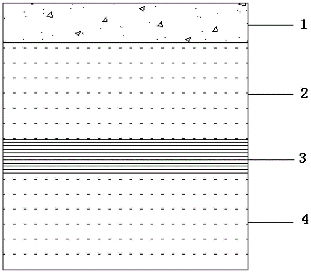
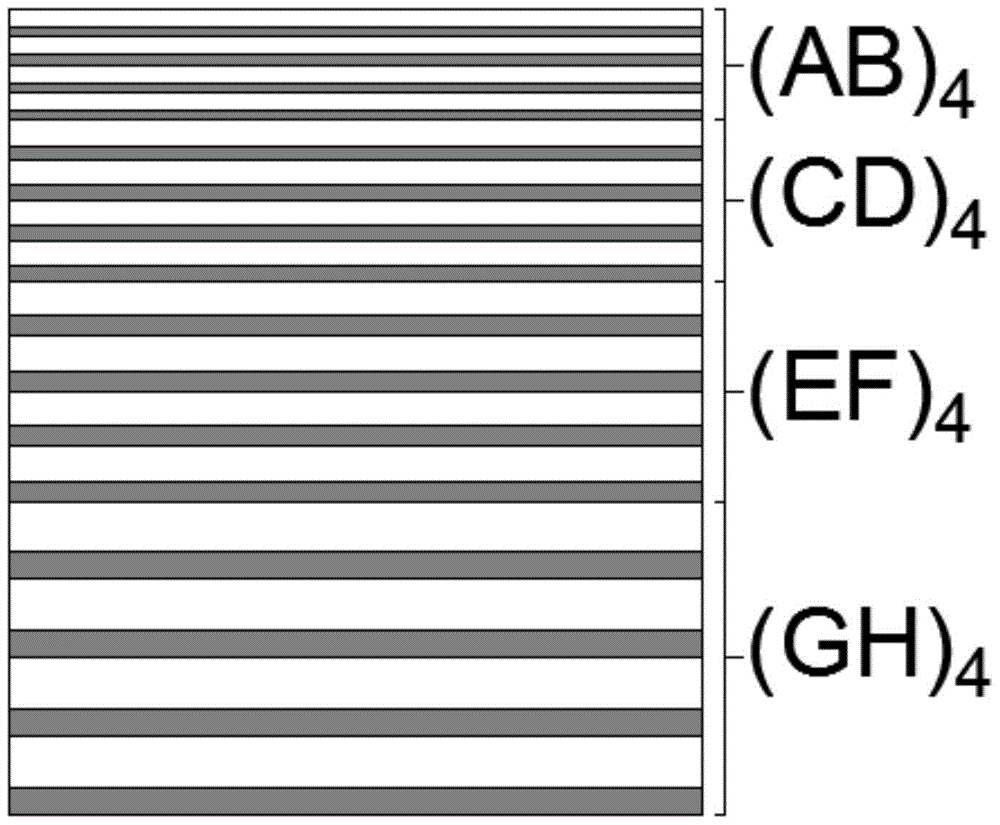
[0035] Such as Figure 1-2As shown, an environmentally friendly cooling film for buildings based on photonic crystals, the cooling film includes a scratch-resistant and wear-resistant layer 1, an upper substrate layer 2, a photonic crystal cooling layer 3 and a lower substrate layer 4 from top to bottom, The anti-scratch and wear-resistant layer 1 is a polyurethane anti-scratch and wear-resistant layer, the upper substrate layer 2 and the lower substrate layer 4 are both polyethylene terephthalate substrate layers, and the photonic crystal cooling layer 3 is composed of the first composite layer , the second composite layer, the third composite layer and the fourth composite layer are stacked sequentially from top to bottom, and the structural formula is (AB) 4 (CD) 4 (EF) 4 (GH) 4 , the first composite layer is composed of 4 layers of A dielectric layer and 4 layers of B dielectric layer alternately superimposed on each other (AB) 4 Type composite structure, the second co...

Embodiment 2

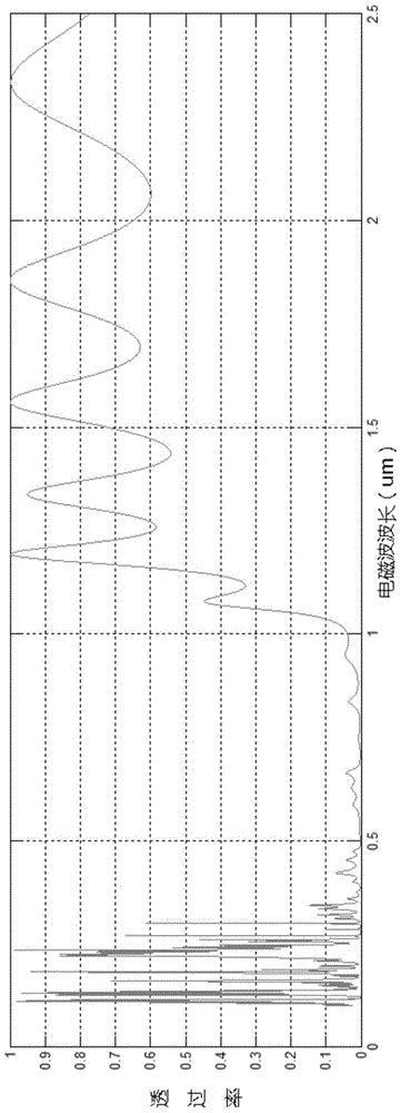
[0042] In this embodiment, the total thickness of the photonic crystal cooling layer 3 is 2.352 μm, the refractive index of the silicon dioxide dielectric layer is 1.45, the titanium dioxide is anatase titanium dioxide, and the refractive index of the anatase titanium dioxide is 2.65.

[0043] The thickness of the A dielectric layer in the first composite layer is 52nm, the thickness of the B dielectric layer is 29nm; the thickness of the C dielectric layer in the second composite layer is 76nm, and the thickness of the D dielectric layer is 42nm; the E dielectric layer in the third composite layer The thickness of the F medium layer is 104nm, the thickness of the F medium layer is 57nm; the thickness of the G medium layer in the fourth composite layer is 147nm, and the thickness of the H medium layer is 81nm; the thickness of the scratch-resistant and wear-resistant layer 1 is 4μm; the upper substrate layer 2 It is equal to the thickness of the lower substrate layer 4, and the...

Embodiment 3

[0045] In this embodiment, the total thickness of the photonic crystal cooling layer 3 is 2.336 μm, the refractive index of the silicon dioxide dielectric layer is 1.45, the titanium dioxide is anatase titanium dioxide, and the refractive index of the anatase titanium dioxide is 2.65.

[0046] The thickness of the A dielectric layer in the first composite layer is 51.5nm, the thickness of the B dielectric layer is 28.5nm; the thickness of the C dielectric layer in the second composite layer is 75.5nm, and the thickness of the D dielectric layer is 41.5nm; the third composite layer The thickness of the medium E medium layer is 103.5nm, the thickness of the F medium layer is 56.5nm; the thickness of the G medium layer in the fourth composite layer is 146.5nm, and the thickness of the H medium layer is 80.5nm; the thickness of the scratch-resistant and wear-resistant layer 1 is 3 μm; the thickness of the upper substrate layer 2 and the lower substrate layer 4 are equal, and the th...


PUM

PropertyMeasurementUnit
thicknessaaaaaaaaaa
thicknessaaaaaaaaaa
thicknessaaaaaaaaaa

Abstract

The invention relates to a photonic crystal-based environment-friendly refrigeration sticker for buildings. The refrigeration sticker sequentially comprises a scratch-resistant wear-resisting layer, an upper base material layer, a photonic crystal refrigeration layer and a lower base material layer from top to bottom, wherein the structural formula of the photonic crystal refrigeration layer is (AB)4(CD)4(EF)4(GH)4; the photonic crystal refrigeration layer is formed by sequentially stacking a first composite layer, a second composite layer, a third composite layer and a fourth composite layer from top to bottom; the first composite layer, the second composite layer, the third composite layer and the fourth composite layer are respectively formed by alternate stacking and combination of four silicon dioxide medium layers and four titanium dioxide medium layers. Compared with the prior art, the photonic crystal-based environment-friendly refrigeration sticker is lightweight and thin, most of electromagnetic waves in sunlight can be reflected through a thin-film structure parameter design by utilizing a one-dimensional photonic crystal band gap principle; and meanwhile, the photonic crystal-based environment-friendly refrigeration sticker almost has no influence on outward thermal radiation in the buildings, and is good in refrigeration effect, beneficial to reduction of energy consumption, and environment-friendly when being applied to building walls.

Description

technical field [0001] The invention belongs to the technical field of one-dimensional photonic crystals, and relates to a cooling film, in particular to an environmentally friendly cooling film for buildings based on photonic crystals. Background technique [0002] More than 99% of the solar radiation spectrum in the upper boundary of the earth's atmosphere is between the wavelength of 0.15-4.0 microns, about 50% of the solar radiation energy is in the visible spectrum (wavelength 0.4-0.76 microns), and 7% is in the ultraviolet spectrum (wavelength <0.4 microns), 43% in the infrared spectral region (wavelength > 0.76 microns), and the maximum energy is at a wavelength of 0.475 microns. Therefore, if the radiant energy of sunlight can be selectively cut off, the purpose of cooling the room can be achieved. At present, in most cases, the cooling of buildings is mainly realized by air conditioning, which consumes a lot of energy. For example, the external walls of buil...

Claims


Application Information

Patent Timeline
Patent Type & Authority Patents(China)
IPC IPC(8): B32B27/08B32B27/36B32B27/40B32B9/04E04B1/74E04B1/92
Inventor 谈论李志远张志华
Owner TONGJI UNIV
Why Eureka
Try Eureka