
A weak magnetic detection device based on 2d artificial magnon crystals
A magnon and magnetic detection technology, which is applied in the directions of magnetic resonance measurement and the size/direction of the magnetic field, can solve the problems of the absorption peak shift of the surface magnetostatic wave, and achieve the effects of simple structure, improved sensitivity and accuracy, and abundant resources
Patent Information
- Authority / Receiving Office
- CN · China
- Patent Type
- Patents(China)
- Current Assignee / Owner
- Publication Date
- 2018-03-27
Smart Images
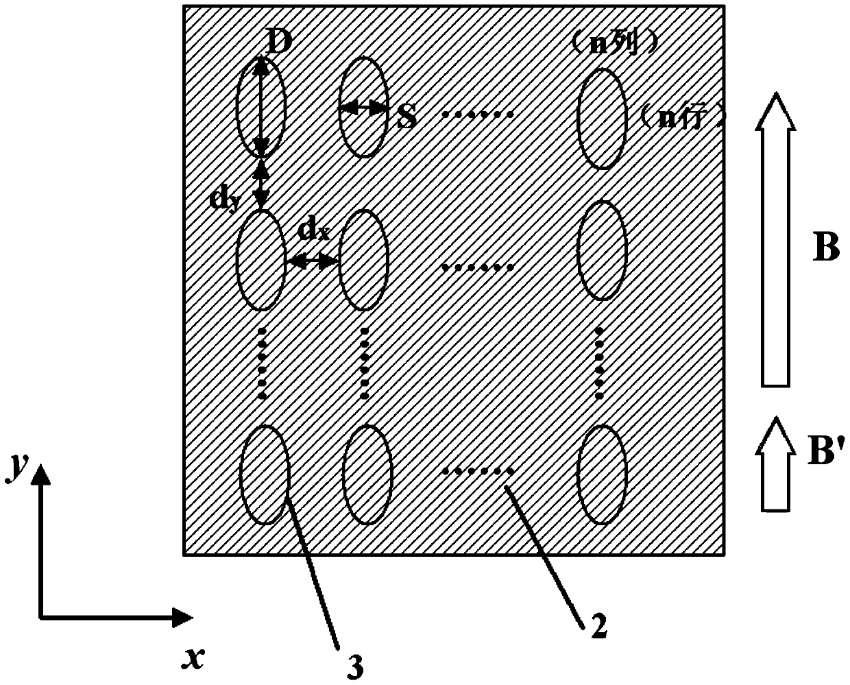
Figure 1 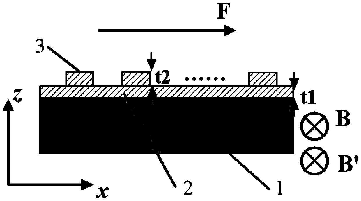
Figure 2 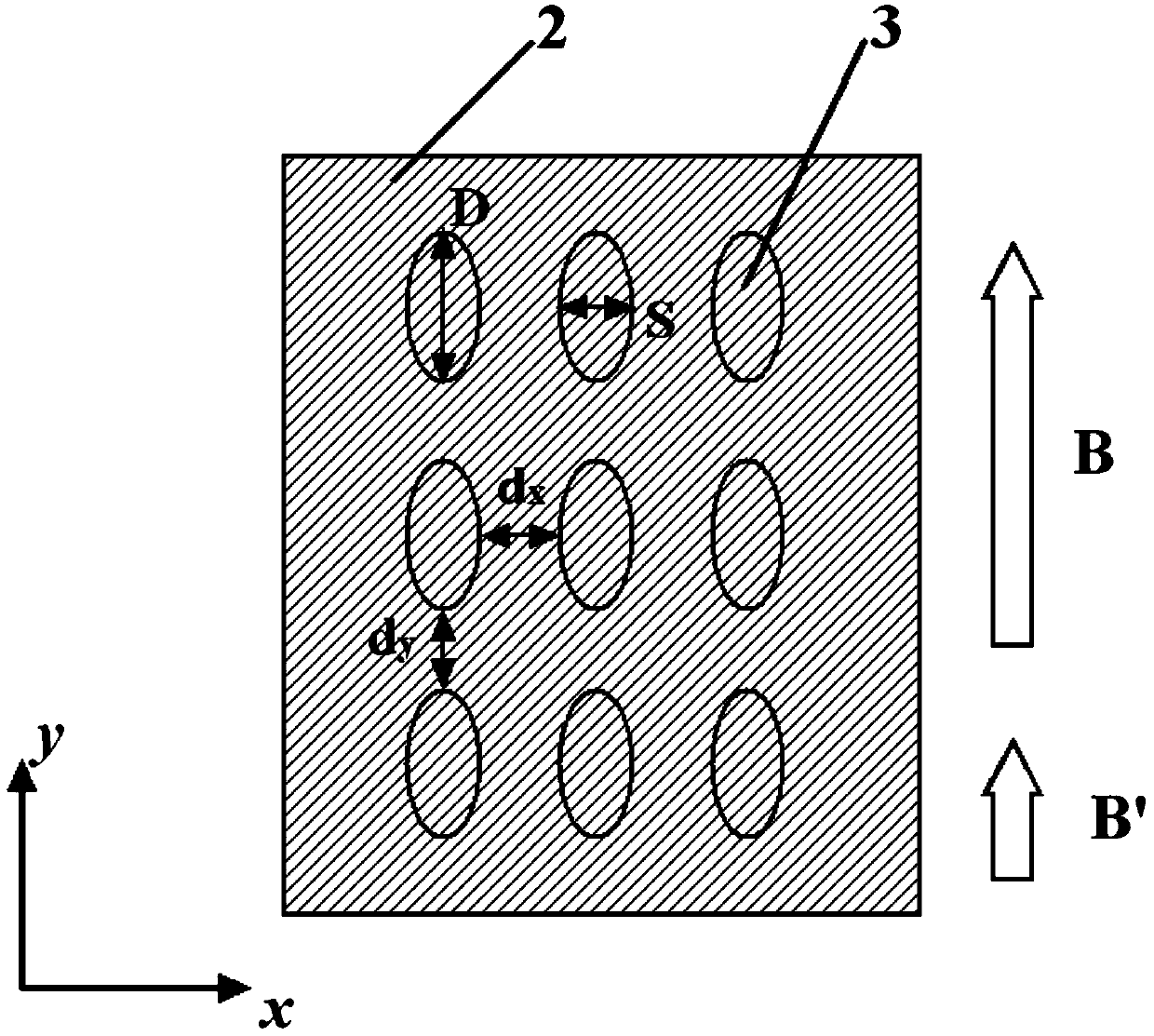
Figure 3
Abstract
Description
technical field
[0001] The invention belongs to the technical field of weak magnetic detection and ferromagnetic materials, in particular to a weak magnetic detection device based on 2D artificial magnon crystals. Background technique
[0002] Weak magnetic detection is one of the important key technologies in the fields of national defense, medical treatment, communication, industry and engineering. Ultra-high-sensitivity magnetic sensors are required to accurately detect weak signal changes of detection objects. A magnon crystal is a periodic artificial magnetic microstructure material that can carry or regulate the propagation of spin waves. It is similar to a photonic crystal and is a special type of artificial crystal. It can be applied to ultra-high sensitivity in the field of weak magnetic detection. sensor element. In recent years, the study of collective spin wave propagation behavior in various periodically structured magnon crystal devices has attracted more and...
Examples
preparation example Construction
[0034] A method for preparing a weak magnetic detection device based on 2D artificial magnon crystals, comprising the following steps:
[0035] 1) The non-magnetic single crystal substrate is ultrasonically rinsed with acetone or ethanol, and then cleaned with deionized water. The selection of materials for the non-magnetic single crystal substrate and the ferromagnetic thin film layer 2 should meet the requirements of material growth kinetics (ie: lining The lattice parameters of the bottom material and the ferromagnetic thin film layer material need to match or be close);
[0036] 2) Using physical or chemical methods such as magnetron sputtering, pulsed laser deposition or chemical vapor deposition, to prepare a ferromagnetic thin film layer 2 on a non-magnetic single crystal substrate;
[0037] 3) An array of patterned ferromagnetic elements 3 arranged periodically is prepared on the ferromagnetic thin film layer 2 by photolithography or ion beam etching.
[0038] The ann...
Embodiment 1
[0040] Figure 2a with Figure 2b They are schematic diagrams of top-view and bottom-view structures implementing a 3×3 array 2D magnon crystal weak magnetic detection device, respectively.
[0041] Such as Figure 2a with Figure 2b As shown, the material of the non-magnetic substrate 1 is a 500 μm thick single polished (100) silicon wafer with a natural oxide layer on the surface. The ferromagnetic thin film layer 2 is made of permalloy soft ferromagnetic material, and the thickness t1 of the thin film layer is 5 nm. The material of the periodically arranged patterned ferromagnetic element 3 array is also made of permalloy, and the periodic arrangement is realized in a 3×3 lattice structure. The width S of the short side and the width D of the long side are both 80 nm, and the thickness t2 is 5 nm. , and the short-side distance dx and long-side distance dy between two adjacent elements are both 10 nm.
[0042] The device is placed in a constant bias magnetic field envir...
Embodiment 2
[0047] Figure 2a with Figure 2b They are schematic diagrams of top-view and bottom-view structures implementing a 3×3 array 2D magnon crystal weak magnetic detection device, respectively.
[0048] Such as Figure 2a with Figure 2b As shown, the material of the non-magnetic substrate 1 is a 500 μm thick single polished (100) silicon wafer with a natural oxide layer on the surface. The ferromagnetic thin film layer 2 is made of permalloy soft ferromagnetic material, and the thickness t1 of the thin film layer is 5 nm. The material of the periodically arranged patterned ferromagnetic element 3 array is also made of Permalloy, and the periodic arrangement is realized in a 3×3 lattice structure. The width S of the short side is 60 nm, the width D of the long side is 80 nm, and the thickness t2 is 5 nm, and the short-side distance dx and long-side distance dy between two adjacent elements are both 10 nm.
[0049] The device is placed in a constant bias magnetic field environ...