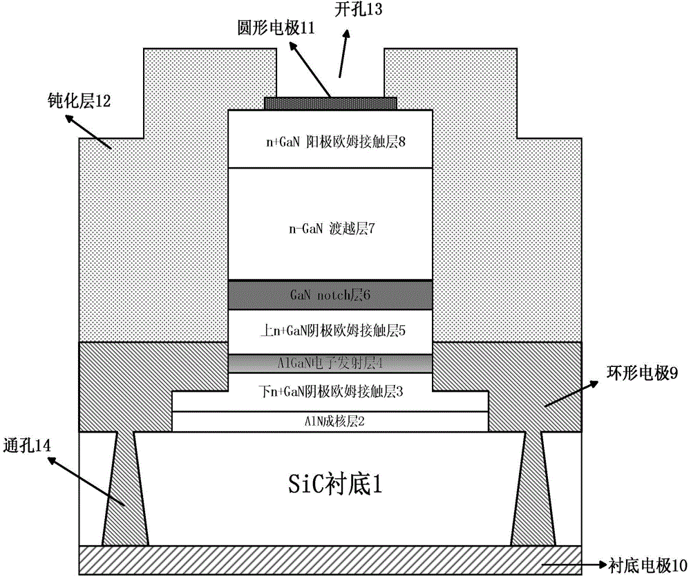
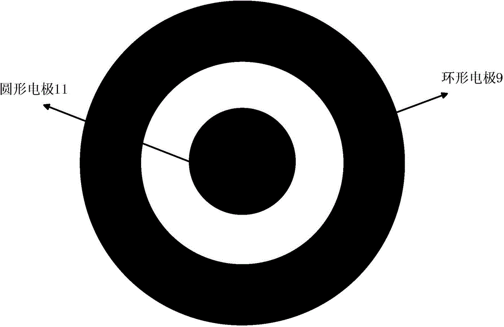
GaN Gunn diode based on notch structure and manufacturing method for GaN Gunn diode
A Gunn diode and cathode technology, which is applied in the field of microelectronic devices, can solve the problems of affecting the electrical characteristics of the device, high dislocation concentration of bulk materials, etc., and achieve the effect of improving the working frequency and conversion efficiency
- Summary
- Abstract
- Description
- Claims
- Application Information
AI Technical Summary
Problems solved by technology
Method used
Image

Examples
Embodiment 1
[0045] Embodiment 1: Fabricate a GaN Gunn diode on a 4H-SiC conductive substrate.
[0046] Step 1, thinning the substrate.
[0047] A 4H-SiC conductive substrate with a diameter of 2 inches is selected, and the back surface is thinned until the thickness of the substrate is 150um.
[0048] Step 2, epitaxially growing an AlN nucleation layer.
[0049] Using MOCVD, under the conditions of maintaining a pressure of 40Torr and a temperature of 650°C, trimethylaluminum and nitrogen are fed simultaneously to grow an AlN nucleation layer with a thickness of 10nm on a 4H-SiC conductive substrate.
[0050] Step 3, epitaxial growth under n + GaN cathode ohmic contact layer.
[0051] Using MOCVD, the temperature is raised to 1060°C, and under the condition of maintaining a pressure of 40Torr, trimethylgallium, nitrogen and n-type dopant source - silane are introduced at the same time, the epitaxial growth thickness is 240nm, and the doping concentration is 1.5×10 18 cm -3 next n +...
Embodiment 2
[0082] Embodiment 2: Fabricate a GaN Gunn diode on a 4H-SiC semi-insulating substrate.
[0083] Step 1, select a 4H-SiC semi-insulating substrate with a diameter of 2 inches, and thin the back surface until the thickness of the substrate is 150um.
[0084] Step 2, put the 4H-SiC semi-insulating substrate into the MOCVD reaction chamber, set the growth temperature to 600°C, feed trimethylaluminum and nitrogen into the reaction chamber at the same time, and grow under the condition of maintaining the pressure at 40 Torr AlN nucleation layer with a thickness of 8 nm.
[0085] Step 3: Raise the substrate on which the AlN nucleation layer has been grown to 1000°C, simultaneously inject trimethylgallium, nitrogen and n-type dopant source-silane into the reaction chamber, and keep the pressure at 40Torr , with a growth thickness of 200nm and a doping concentration of 1.0×10 18 cm -3 next n + GaN cathode ohmic contact layer.
[0086] Step 4, the pressure in the MOCVD reaction cha...
Embodiment 3
[0099] Embodiment 3: Fabricate a GaN Gunn diode on a 6H-SiC conductive substrate.
[0100] Step A, thinning the substrate.
[0101] A 6H-SiC conductive substrate with a diameter of 2 inches is selected, and the back surface is thinned until the thickness of the substrate is 150um.
[0102] Step B, making AlN nucleation layer and lower n + GaN cathode ohmic contact layer.
[0103] In the MOCVD reaction chamber, under the conditions of keeping the pressure at 60 Torr and the temperature at 650°C, feed trimethylaluminum and nitrogen at the same time, and grow an AlN nucleation layer with a thickness of 10nm on the 6H-SiC conductive substrate; continue Using MOCVD process, raise the temperature to 1100℃, keep the pressure at 60Torr, and then pass trimethylgallium, nitrogen and n-type doping source-silane at the same time, the epitaxial growth thickness is 300nm, and the doping concentration is 2×10 18 cm -3 next n + GaN cathode ohmic contact layer.
[0104] Step C, epitaxial...
PUM
 Abstract
Description
Claims
Application Information