Semiconductor device
A technology of semiconductor and oxide semiconductor, which is applied in the direction of semiconductor devices, semiconductor/solid-state device manufacturing, transistors, etc., can solve the problem of high contact resistance, achieve the effect of suppressing the reduction of adhesion and improving the yield
- Summary
- Abstract
- Description
- Claims
- Application Information
AI Technical Summary
Problems solved by technology
Method used
Image
Examples
no. 1 approach
[0043]Hereinafter, a first embodiment of the semiconductor device of the present invention will be described with reference to the drawings. The semiconductor device of this embodiment includes an oxide semiconductor TFT. In addition, the semiconductor device according to the present embodiment only needs to include an oxide semiconductor TFT, and broadly includes active matrix substrates, various display devices, electronic equipment, and the like.
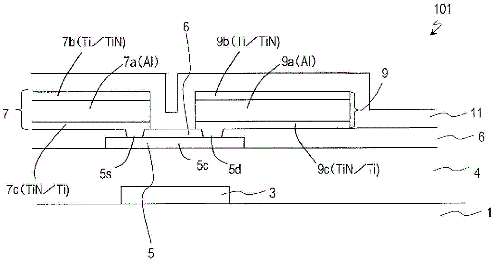
[0044] figure 1 It is a schematic cross-sectional view of the oxide semiconductor TFT 101 of this embodiment.
[0045] The oxide semiconductor TFT 101 includes: a gate electrode 3 supported on a substrate 1; a gate insulating layer 4 covering the gate electrode 3; semiconductor layer 5 ; and source electrode 7 and drain electrode 9 . The oxide semiconductor layer 5 has a channel region 5c, and source contact regions 5s and drain electrode contact regions 5d located on both sides of the channel region. The source electrode 7 i...
no. 2 approach
[0112] In the oxide semiconductor TFT of this embodiment mode, the layers located on the side of the oxide semiconductor layer among the lower and upper layers of the source and drain electrodes further have another metal nitride layer between the metal layer and the oxide semiconductor layer. In terms of the above-mentioned oxide semiconductor TFT 101 ( figure 1 )different.
[0113] Figure 6 It is a cross-sectional view illustrating an oxide semiconductor TFT 102 according to the second embodiment of the present invention.
[0114] The lower layers 7 c and 9 c of the source and drain electrodes of the oxide semiconductor TFT 102 of this embodiment further include a TiN layer on the side opposite to the main layers 7 a and 9 a of the Ti layer. Therefore, the lower layers 7c, 9c are laminated films including a TiN layer, a Ti layer, and a TiN layer in this order from the main layer 7a, 9a side. That is, it has a three-layer structure of TiN / Ti / TiN. In this example, the TiN...
no. 3 approach
[0124] The upper layer of the source and drain electrodes of the oxide semiconductor TFT of this embodiment further has another metal nitride layer between the metal film and the first protective layer, and in this respect is different from the above-mentioned oxide semiconductor TFT 101 ( figure 1 )different.
[0125] Figure 7 It is a cross-sectional view of an oxide semiconductor TFT 103 according to a third embodiment of the present invention.
[0126] The upper layers 7 b and 9 b of the source electrode and the drain electrode of the oxide semiconductor TFT 103 of this embodiment further include a TiN layer on the side of the Ti layer opposite to the main layers 7 a and 9 a. Therefore, the upper layers 7b, 9b are laminated films including a TiN layer, a Ti layer, and a TiN layer in this order from the main layer 7a, 9a side. That is, it has a three-layer structure of TiN / Ti / TiN. In this example, the uppermost TiN layer of the upper layers 7 b , 9 b is in contact with t...
PUM
| Property | Measurement | Unit |
|---|---|---|
| thickness | aaaaa | aaaaa |
| thickness | aaaaa | aaaaa |
| thickness | aaaaa | aaaaa |
Abstract
Description
Claims
Application Information
 - R&D
- Intellectual Property
- Life Sciences
- Materials
- Tech Scout
- Unparalleled Data Quality
- Higher Quality Content
- 60% Fewer Hallucinations
Browse by: Latest US Patents, China's latest patents, Technical Efficacy Thesaurus, Application Domain, Technology Topic, Popular Technical Reports.
© 2025 PatSnap. All rights reserved.Legal|Privacy policy|Modern Slavery Act Transparency Statement|Sitemap|About US| Contact US: help@patsnap.com


