Film packaging structure and organic light-emitting device with same

A thin-film packaging and thin-film technology, which is applied in organic light-emitting devices, organic light-emitting device structures, organic semiconductor devices, etc., can solve the problems of being easily affected by water vapor and oxygen, causing reactions, slow deposition speed, and shortening the service life of devices. Easy control of deposition conditions and thickness, good compactness and uniformity, weight and cost reduction

Inactive Publication Date: 2015-06-17
EVERDISPLAY OPTRONICS (SHANGHAI) CO LTD
View PDF4 Cites 5 Cited by
  • Summary
  • Abstract
  • Description
  • Claims
  • Application Information

AI Technical Summary

Problems solved by technology

[0002] For organic light-emitting diodes (OLEDs), electrons need to be injected from the cathode during operation. The cathode uses metals with low work functions such as aluminum, magnesium, silver, calcium, etc. These metals are relatively active and are susceptible to reactions under the influence of water vapor and oxygen. At the same time, other organic materials in OLED devices are also susceptible to changes due to the influence of water vapor and oxygen, which will cause the properties and performance of these materials to degrade or fail, and eventually lead to a shortened service life of the device. It is very important to efficiently package the device to isolate the functional layers of the device from water vapor, oxygen, etc. in the surrounding environment
[0003] The traditional OLED device packaging is to make electrodes and various functional layers on the substrate glass, and then use the glass substrate with good chemical stability, compactness and electrical insulation as the protective cover of the device to protect the device, but the glass substrate The mechanical properties are poor, cracks and glue breaks are prone to occur, and the requirements for flexible effects cannot be met, and the glass substrate takes up a lot of space, which does not meet the development trend of light and thin OLED devices
[0004] Thin film encapsulation (TFE) technology physically protects devices in the encapsulation area by forming a thin film with a dense structure. It is a gapless encapsulation method and has a better effect of isolating water vapor and oxygen. Thin film encapsulation technology often uses chemical vapor deposition (CVD) technology Forming thin films with atomic layer deposition (ALD) technology, CVD technology and ALD technology use precursors in the reaction process, often involving or releasing harmful gases, there are hidden dangers of harming the environment and human body, and there are problems such as slow deposition speed and complicated process

Method used


Image

  • Film packaging structure and organic light-emitting device with same
  • Film packaging structure and organic light-emitting device with same
  • Film packaging structure and organic light-emitting device with same

Examples


Embodiment 1

[0043] Example 1: Al 2 o 3 -ZrO 2 / SiN package structure

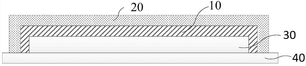
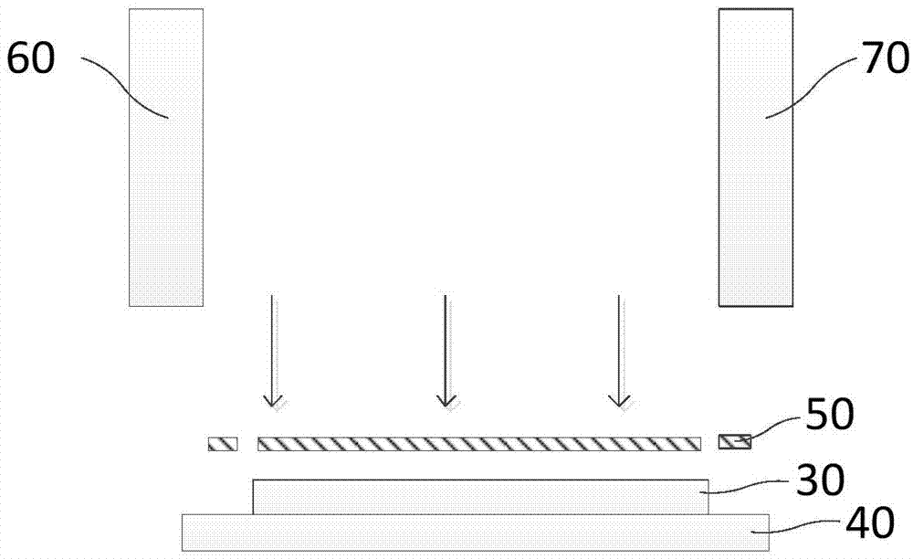
[0044] al 2 o 3 -ZrO 2 Formation of the mixed layer thin film 10: the device 30 takes an OLED unit prepared with electrodes and functional layers as an example, a mask 50 is placed on the device 30, and an amorphous Al 2 o 3 with crystalline ZrO 2 Target sputtering was performed as the first target 60 and the second target 70 respectively, and the sputtering power was set to 300W, the flow rate of argon gas was 30 sccm, the pressure was 1.0 mTorr, the flow rate of oxygen gas was 0.8 sccm, and the deposition time was 30 min. Al formed 2 o 3 -ZrO 2 The thickness of the mixed layer film 10 is about 100nm;

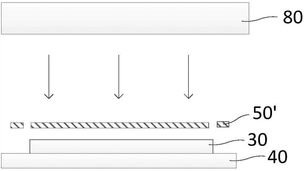
[0045] Formation of the SiN thin film: place the mask 50' above the device 30 on which the mixed layer thin film 10 is deposited, and perform magnetron sputtering with SiN as the third target 80, set the sputtering power to 500W, and the argon gas flow rate to 30 sccm, The pressure is 0.9mTorr, and the depo...

Embodiment 2

[0047] Example 2: Al 2 o 3 -ZnO / SiN package structure

[0048] al 2 o 3 -Formation of ZnO mixed layer thin film 10: device 30 takes an OLED unit prepared with electrodes and functional layers as an example, place mask 50 above device 30, and use amorphous Al 2 o 3 and crystalline ZnO as the first target 60 and the second target 70 respectively for target sputtering, set the sputtering power to 300W, the argon gas flow to 30sccm, the pressure to 1.0m Torr, the oxygen flow to 0.8sccm, and the deposition time for 30min. Al formed 2 o 3 - the thickness of the ZnO mixed layer thin film 10 is about 100nm;

[0049] Formation of the SiN thin film: place the mask 50' above the device 30 on which the mixed layer thin film 10 is deposited, and perform magnetron sputtering with SiN as the third target 80, set the sputtering power to 500W, and the argon gas flow rate to 30 sccm, The pressure is 0.9mTorr, and the deposition time is 30min. The formed SiN thin film 20 has a thicknes...

Embodiment 3

[0051] Example 3: Al 2 o 3 -MgO / Si 3 N 4 Package structure

[0052] al 2 o 3 -Formation of the MgO mixed layer thin film 10: the device 30 takes the OLED unit prepared with electrodes and functional layers as an example, the mask 50 is placed on the device 30, and the amorphous Al 2 o 3 and crystalline MgO respectively as the first target 60 and the second target 70 for target sputtering, set the sputtering power to 300W, the argon gas flow to 30sccm, the pressure to 1.0Torr, the oxygen flow to 0.8sccm, and the deposition time to be 30min. Al formed 2 o 3 - the thickness of the MgO mixed layer thin film 10 is about 110nm;

[0053] Si 3 N 4 Formation of the thin film: the mask 50' is placed over the device 30 deposited with the mixed layer thin film 10, with Si 3 N 4 Magnetron sputtering is performed for the third target 80 , the sputtering power is set to 500W, the argon gas flow rate is 30 sccm, the pressure is 0.9mTorr, and the deposition time is 30min. Formed...


PUM

PropertyMeasurementUnit
thicknessaaaaaaaaaa
thicknessaaaaaaaaaa

Abstract

The invention provides a film packaging structure used for packaging functional devices on a substrate. The film packaging structure comprises a mixed layer film covering the functional devices and an inorganic layer film located on the mixed layer film. The mixed layer film is mainly composed of amorphous aluminum oxide and crystalline oxide. The invention further provides an organic light-emitting device including the substrate, an OLED on the substrate and the film packaging structure. A protective film composed of the mixed layer film and the inorganic layer film is firm and good in airtightness and uniformity, an effective packaging effect can be realized, the device weight and cost are remarkably reduced, any chemical gas exists or is released when the mixed layer film and the inorganic layer film deposit through the sputtering technology, the environment is free of threats, and environment-friendly packaging is realized.

Description

technical field [0001] The invention relates to an electronic device packaging structure, in particular to a thin film packaging structure and an organic light-emitting device with the structure. Background technique [0002] For organic light-emitting diodes (OLEDs), electrons need to be injected from the cathode during operation. The cathode uses metals with low work functions such as aluminum, magnesium, silver, calcium, etc. These metals are relatively active and are susceptible to reactions under the influence of water vapor and oxygen. At the same time, other organic materials in OLED devices are also susceptible to changes due to the influence of water vapor and oxygen, which will cause the properties and performance of these materials to degrade or fail, and eventually lead to a shortened service life of the device. Efficient packaging of devices is crucial to isolate each functional layer of the device from water vapor, oxygen, etc. in the surrounding environment. ...

Claims


Application Information

Patent Timeline
Patent Type & Authority Applications(China)
IPC IPC(8): H01L51/52H01L51/56
CPCH10K50/84H10K2102/00H10K2102/302H10K50/844H10K71/00C23C14/3464C23C14/0652C23C14/081C23C14/08H10K50/846H01L21/02266H01L21/02178H01L21/022
Inventor 肖玲李贵芳胡妞
Owner EVERDISPLAY OPTRONICS (SHANGHAI) CO LTD
Why Eureka
Try Eureka