Method for fabricating surface-enhanced Raman scattering substrates with metal nanogap using ALD

A surface-enhanced Raman and metal nanotechnology, which is applied in Raman scattering, metal material coating technology, gaseous chemical plating, etc., can solve the problems of poor stability and repeatability, difficulty in preparing micro-nano structures in large areas, and high production costs and other problems, to achieve the effect of simple steps, good repeatability and low cost

Active Publication Date: 2017-10-03
NANJING UNIV
View PDF4 Cites 3 Cited by
  • Summary
  • Abstract
  • Description
  • Claims
  • Application Information

AI Technical Summary

Problems solved by technology

[0005] At present, most of the SERS substrates prepared by chemical methods are disordered structures. Although the preparation method is simple and can obtain a large enhancement factor, the stability and repeatability are poor; physical methods such as electron beam exposure, ion beam etching and other technologies are used. Ordered structures with good repeatability can be prepared, but the production cost is high, and it is difficult to prepare micro-nano structures in large areas

Method used


Image

  • Method for fabricating surface-enhanced Raman scattering substrates with metal nanogap using ALD
  • Method for fabricating surface-enhanced Raman scattering substrates with metal nanogap using ALD
  • Method for fabricating surface-enhanced Raman scattering substrates with metal nanogap using ALD

Examples


Embodiment 1

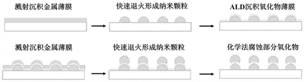
[0031] (1) figure 1 Is a flow chart of the method of the present invention, such as figure 1 As shown, the silicon wafer was ultrasonically cleaned with acetone, isopropanol, ethanol, and deionized water for 5 minutes, respectively.

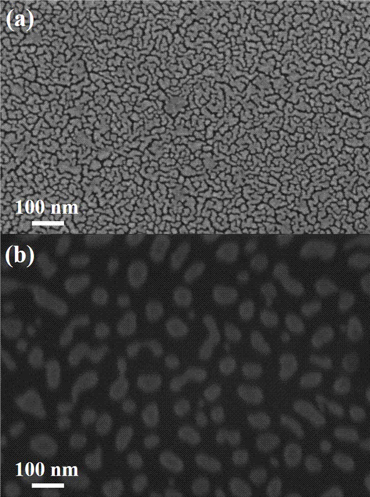
[0032] (2) Transfer the cleaned substrate to the magnetron sputtering reaction chamber, and deposit about 3nm Au thin film, figure 2 (A) is the SEM image of the Au thin film; under a nitrogen atmosphere, the Au thin film is subjected to rapid annealing at 500° C. for 30 seconds to generate Au nanoparticles; figure 2 (B) is the SEM image of Au nanoparticles.

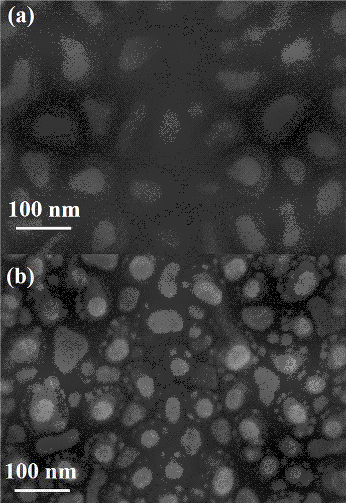
[0033] (3) Transfer the Au nanoparticle substrate obtained in step 2 to the ALD reaction chamber, and deposit 2nm, 10nm and 20nm Al respectively 2 O 3 Thin film, forming Al 2 O 3 Wrapped gold nanoparticle structure, image 3 (A) For wrapping 20nmAl 2 O 3 SEM image of the gold nanoparticle structure of the film.

[0034] ALD deposited Al 2 O 3 The parameters are:

[0035] Reaction chamber temperat...

Embodiment 2

[0042] (1) Wash the quartz glass with acetone, isopropanol, ethanol and deionized water, respectively, ultrasonically for 5 minutes;

[0043] (2) Transfer the cleaned substrate to the electron beam evaporation reaction chamber, and deposit a silver film of about 5nm; in a nitrogen atmosphere, the silver film is subjected to rapid annealing at 500 ℃ for 50 seconds to generate silver nanoparticles;

[0044] (3) Transfer the substrate with silver nanoparticles to the ALD reaction chamber, and grow a 5nm zinc oxide film to form zinc oxide-coated silver nanoparticles;

[0045] The parameters of ALD deposition of zinc oxide are:

[0046] Reaction chamber temperature 150 o C, with Zn(C 2 H 5 ) 2 And H 2 O is the reaction source, first pass in Al(CH 3 ) 3 Pulse 0.1s, followed by high-purity nitrogen pulse cleaning for 4s to wash away the reaction by-products and residual reaction sources, and finally water vapor pulse for 0.1s; the above is a cycle of atomic layer deposition, according to the ...

Embodiment 3

[0051] (1) Wash the silicon wafers with acetone, isopropanol, ethanol, and deionized water, respectively, ultrasonically for 5 minutes;

[0052] (2) Transfer the cleaned substrate to the ALD reaction chamber, and deposit 100 cycles of Pt nanoparticles with a thickness of about 5nm. The resulting Pt nanoparticles are as Figure 8 Shown.

[0053] The parameters of ALD deposition of Pt are:

[0054] Reaction chamber temperature 300 o C, to PtMeCpMe 3 And O 2 As the reaction source, PtMeCpMe 3 The source temperature is 70 o C; access to PtMeCpMe first 3 Pulse 0.2s, followed by nitrogen pulse cleaning for 4s, then pass O 2 The pulse is 1.5s, and finally high-purity nitrogen is pulsed and flushed for 20s; the above is a cycle of atomic layer deposition. According to the desired thickness of the Pt film, the cycle is repeated. In this embodiment, a total of 100 cycles are performed.

[0055] (3) Then deposit 5 nm SiO in the ALD reaction chamber 2 Thin film, forming Pt nanoparticle structure ...


PUM

PropertyMeasurementUnit
thicknessaaaaaaaaaa
thicknessaaaaaaaaaa

Abstract

The invention discloses a method for preparing surface-enhanced Raman scattering base with metal nanometer gaps by utilizing ALD (atomic layer deposition). The method specifically comprises the following steps: (a) washing a substrate; (b) generating metal nanometer particles on the surface of the substrate; and (c) depositing a layer of oxide film on the surface of the substrate; (d) depositing metal nano particles on the surface of the substrate; (e) placing the substrate in an acid solution or an alkaline solution to be corroded to obtain the surface-enhanced Raman scattering base with metal nanometer gaps. Oxide with uniform nanoscale thickness is introduced among metal particles by utilizing ALD, and a part of oxide is removed through a chemical corrosion method so that nanoscale metal gaps are prepared and the surface-enhanced Raman scattering base is prepared. The method is simple in steps, good in repeatability and low in cost, and the obtained substrate has excellent surface-enhanced Raman scattering performance.

Description

Technical field [0001] The invention relates to the field of molecular recognition and micro-nano composite structure preparation, in particular to a method for preparing a metal nano-gap surface enhanced Raman scattering substrate by using ALD. Background technique [0002] Raman spectroscopy is a spectroscopic technique for studying molecular vibrational energy levels, which is widely used in the field of molecular recognition. However, ordinary Raman spectroscopy signals are very weak and difficult to detect, which limits its application in actual production. Surface-enhanced Raman scattering (SERS) spectroscopy technology realizes several orders of magnitude enhancement of ordinary Raman signals by constructing a substrate with a special surface, thereby effectively detecting low-concentration molecules. It is a trace analysis with great application prospects. technology. [0003] The Surface Enhanced Raman Scattering Effect (SERS) was discovered in the mid-1970s. This effect ...

Claims


Application Information

Patent Timeline
Patent Type & Authority Patents(China)
IPC IPC(8): C23C16/455C23C16/40C23C16/56G01N21/65
Inventor 李爱东曹燕强朱琳曹正义吴迪
Owner NANJING UNIV
Why Eureka
Try Eureka