

Thallium-doped caesium iodide scintillator and application thereof
A technology of thallium cesium iodide and cesium iodide, which is applied to thallium-doped cesium iodide scintillators and its application fields, can solve the problems of reduced light output and damage to the performance advantages of cesium iodide crystals, and achieve low afterglow and high scintillation efficiency effect
- Summary
- Abstract
- Description
- Claims
- Application Information
AI Technical Summary
Problems solved by technology
Method used
Image

Examples
Embodiment 1
[0031] Embodiment 1: preparation (Cs 0.9985 Tl 0.001 Yb 0.0005 )(I 1.0005 )film
[0032] 259.25g CsI, 0.33125g TlI and 0.2134g YbI 2 After fully mixing, put it into a molybdenum metal evaporation boat fixed on the electrode, heat the single crystal silicon substrate to 200 ° C by means of resistance heating, and the pressure in the hot steam chamber drops to 10 -2 torr, carry out ion bombardment for more than 10 minutes, rotate the substrate holder during evaporation, stop the evaporation when the film thickness reaches 100 μm, wait for the temperature to drop to 250°C and keep it warm for 25 minutes for annealing, and keep the original pressure for about 8 hours after dropping to room temperature Remove the substrate again.
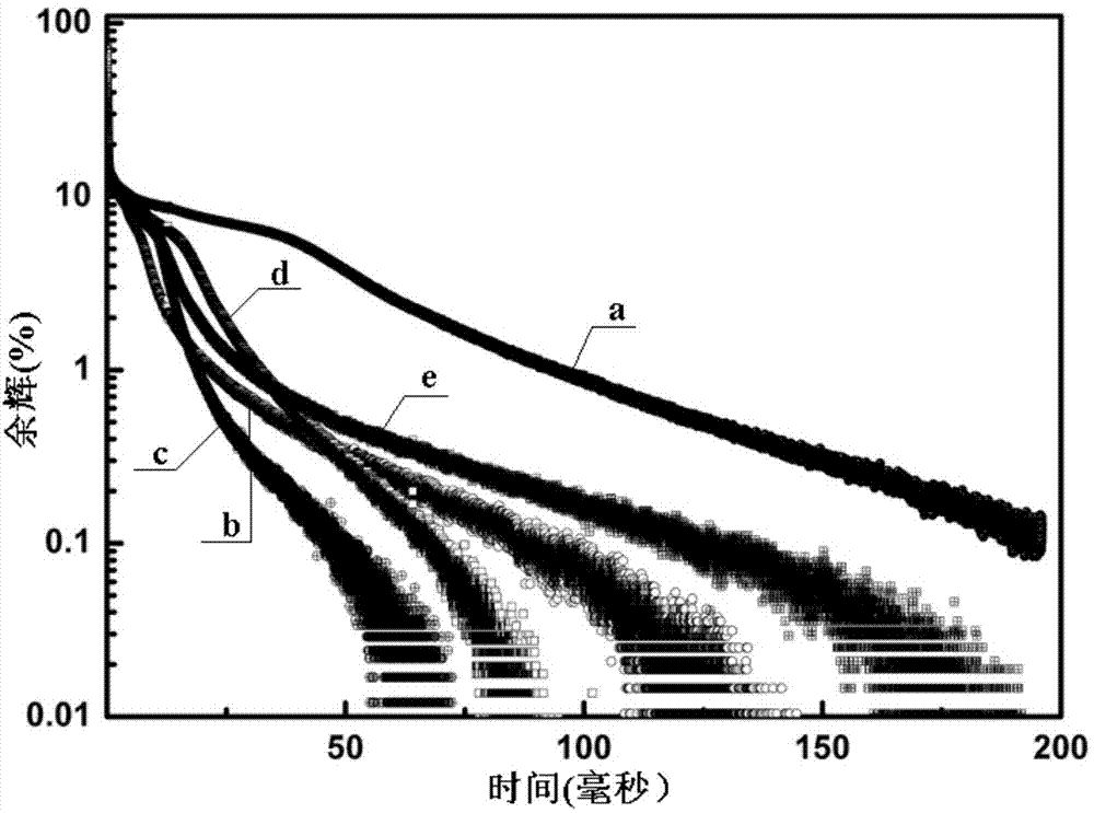
[0033]The grown film sample is colorless and transparent, and is firmly bonded to the substrate. Tested by an X-ray pulse afterglow tester, it is shown that the afterglow of the sample is significantly lower than that of the film sample without co-...
Embodiment 2
[0034] Embodiment 2: preparation (Cs 0.998 Tl 0.001 Yb 0.001 )(I 1.002 )film
[0035] 259.3g CsI, 0.6265g TlI and 0.55375g YbI 3 After fully mixing, put it into a molybdenum metal evaporation boat fixed on the electrode, heat the silicon substrate to 200°C by means of resistance heating, and the pressure in the steam chamber is reduced to 10 -2 torr, carry out ion bombardment for more than 10 minutes, rotate the substrate holder during evaporation, stop the evaporation when the film thickness reaches 200 μm, keep the temperature for 20 minutes after the temperature drops to 200°C and anneal, and keep the original pressure for about 8 hours after cooling down to room temperature Remove the substrate again.
[0036] The grown film sample is colorless and transparent, and is firmly bonded to the substrate. Tested by an X-ray pulse afterglow tester, it is shown that the afterglow of the sample is significantly lower than that of the film sample without co-doped ytterbium ion...
Embodiment 3
[0040] Embodiment 3: preparation (Cs 0.998 Tl 0.001 Yb 0.001 )(I 0.999 Cl 0.002 ) single crystal fiber
[0041] 51.86g CsI, 0.06626g TlI and 0.04879gYbCl 2 After fully mixing, put it into a Ф15mm iridium crucible, fill the growth furnace with high-purity nitrogen, heat the raw material to a molten state, and keep the temperature for 5 hours after the raw material is completely melted. Coil, disconnect the power supply and take out the crystal after cooling down to room temperature.
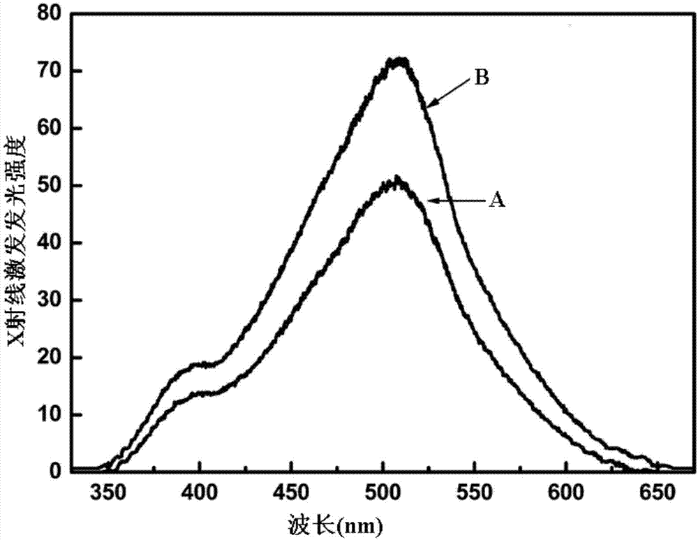
[0042] After cutting, grinding and polishing, the crystal is processed into a crystal sample with a diameter of 3 mm and a length of 1 mm. The grown crystals are colorless and transparent without inclusions. Tested by an X-ray pulse afterglow tester, it is shown that the afterglow of the crystal sample is significantly lower than that of the sample without co-doped ytterbium ions (the sample obtained in Comparative Example 2). X-ray excitation emission spectroscopy test results show that t...
PUM
 Abstract
Description
Claims
Application Information