Preparation method of erbium-doped lithium niobate optical waveguide amplifier
A technology of optical waveguide amplifier and lithium niobate, which is applied in lasers, laser components, instruments, etc.
- Summary
- Abstract
- Description
- Claims
- Application Information
AI Technical Summary
Problems solved by technology
Method used
Image
Examples
Embodiment 1
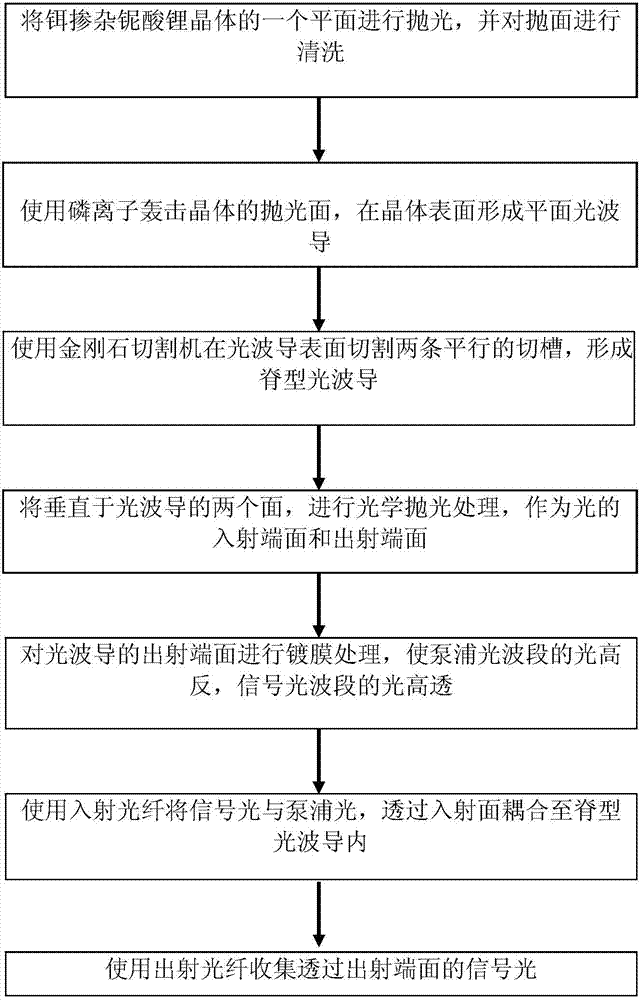
[0027] A preparation method for an erbium-doped lithium niobate optical waveguide amplifier, comprising the following steps:
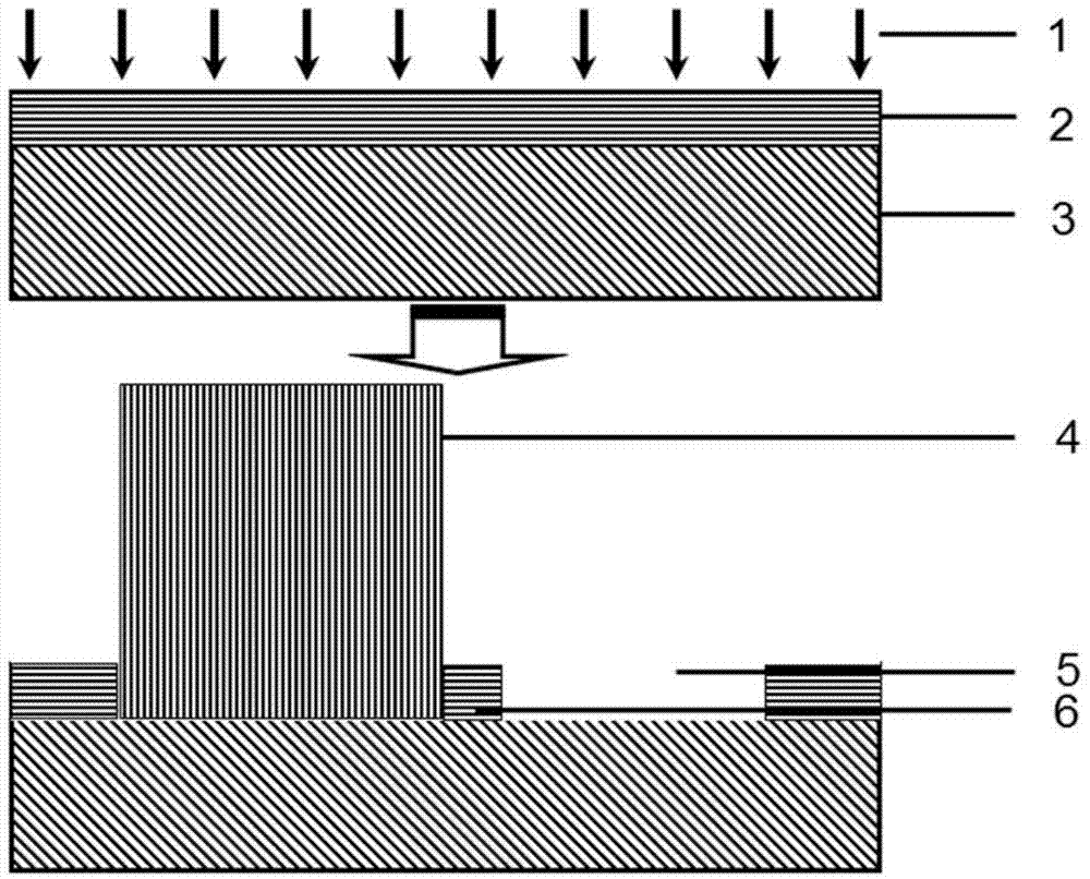
[0028] 1) Optically polishing the surface to be processed of the erbium ion-doped lithium niobate crystal 3, the surface to be processed is perpendicular to the c-axis of the erbium ion-doped lithium niobate crystal 3;
[0029] 2) Utilize the ion beam accelerator to send phosphorus ions, bombard the polished surface of the erbium ion-doped lithium niobate crystal 3, and form a planar optical waveguide 2 on the polished surface of the erbium ion-doped lithium niobate crystal 3;
[0030] 3) processing a ridge-shaped optical waveguide 6 on the surface of the planar optical waveguide 2;
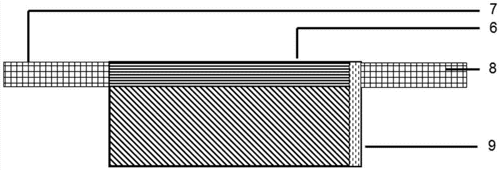
[0031] 4) Optically polishing the two end faces perpendicular to the ridge-shaped optical waveguide 6 as the outgoing end face and the incident end face;
[0032] 5) performing an optical coating on the exit end surface, the optical coating 9 is highly transparent to sig...
Embodiment 2
[0040] A kind of preparation method of erbium-doped lithium niobate optical waveguide amplifier as described in embodiment 1, its difference is,
[0041] In the step 2), the energy of the phosphorus ion is 10 MeV, and the dose is 6×10 15 ions / cm 2 .
[0042] In the step 3), processing the ridge optical waveguide includes: cutting two parallel grooves on the surface of the planar optical waveguide, the depth of the grooves is 30 μm, and the width is 200 μm; the two grooves The spacing between them is 30 μm, forming a ridge waveguide with a width of 30 μm.
[0043] In the step 5), an optical coating is applied to the exit end surface, and the optical coating is highly transparent to signal light with a wavelength range of 1.55 μm and highly reflective to pump light with a wavelength range of 810 nm.
PUM
| Property | Measurement | Unit |
|---|---|---|
| Depth | aaaaa | aaaaa |
| Width | aaaaa | aaaaa |
| Width | aaaaa | aaaaa |
Abstract
Description
Claims
Application Information


