Organic thin-film solar cell based on three emitting layers and preparing method thereof

A technology of solar cells and organic thin films, applied in semiconductor/solid-state device manufacturing, circuits, photovoltaic power generation, etc., can solve the problem of generating photocurrent, unable to solve the problem of excitons quenching and entering the anode or anode modification layer, and unable to form excitons. Sub-transmission and other issues, to achieve the effect of improving photocurrent, improving light absorption efficiency, and increasing utilization efficiency

Inactive Publication Date: 2015-07-08
UNIV OF ELECTRONICS SCI & TECH OF CHINA
View PDF4 Cites 5 Cited by
  • Summary
  • Abstract
  • Description
  • Claims
  • Application Information

AI Technical Summary

Problems solved by technology

[0004] However, this method still cannot solve the quenching of excitons at the interface and enter the anode or anode modification layer. Many excitons are quenched and disappear during the transmission process, and cannot form efficient excitons to transport into the separation interface and generate photocurrent.

Method used


Image

  • Organic thin-film solar cell based on three emitting layers and preparing method thereof
  • Organic thin-film solar cell based on three emitting layers and preparing method thereof
  • Organic thin-film solar cell based on three emitting layers and preparing method thereof

Examples


Embodiment 1

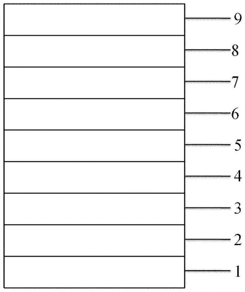
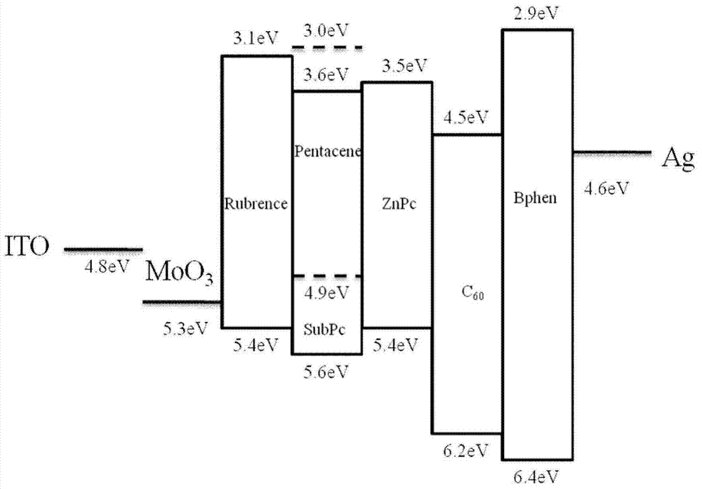
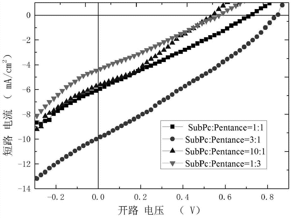
[0048] The structure of organic solar cells such as figure 2 shown. The material, thickness and doping ratio of each layer of the device are as follows: the transparent substrate is glass, the transparent anode electrode is ITO, and the thickness is 180nm; the anode modification layer is MoO 3 , the thickness is 10nm; the first donor layer is Rubrene, the thickness is 5nm; the second donor layer is SubPc: Pentance=10:1, the thickness is 7nm; the third donor layer is ZnPc, the thickness is 5nm; the acceptor layer for C 60 , the thickness is 30nm; the electronic buffer layer is Bphen, the thickness is 5nm; the cathode electrode is Ag, the thickness is 130nm.

[0049] Its preparation method is as follows:

[0050] ① The glass substrate on which the transparent anode electrode ITO has been sputtered is ultrasonically cleaned with detergent, deionized water, acetone solution and ethanol solution, and dried with dry nitrogen after cleaning;

[0051] ② Move the above-mentioned I...

Embodiment 2

[0060] The structure of organic solar cells such as figure 2 shown. The material, thickness and doping ratio of each layer of the device are as follows: the transparent substrate is glass, the transparent anode electrode is ITO, and the thickness is 180nm; the anode modification layer is MoO 3 , the thickness is 10nm; the first donor layer is Rubrene, the thickness is 5nm; the second donor layer is SubPc: Pentance=3:1, the thickness is 7nm; the third donor layer is ZnPc, the thickness is 5nm; the acceptor material Layer is C 60 , the thickness is 30nm; the electronic buffer layer is Bphen, the thickness is 5nm; the cathode electrode is Ag, the thickness is 130nm. The preparation process is basically similar to Example 1.

Embodiment 3

[0062] The structure of organic solar cells such as figure 2 shown. The material, thickness and doping ratio of each layer of the device are as follows: the transparent substrate is glass, the transparent anode electrode is ITO, and the thickness is 180nm; the anode modification layer is MoO 3 , the thickness is 10nm; the first donor layer is Rubrene, the thickness is 5nm; the second donor layer is SubPc: Pentance=1:3, the thickness is 7nm; the third donor layer is ZnPc, the thickness is 5nm; the acceptor material Layer is C 60 , the thickness is 30nm; the electronic buffer layer is Bphen, the thickness is 5nm; the cathode electrode is Ag, the thickness is 130nm. The preparation process is basically similar to Example 1.


PUM


Abstract

The invention discloses an organic thin-film solar cell based on three emitting layers and a preparing method thereof. The organic thin-film solar cell is of a regular structure and sequentially comprises a transparent substrate, a transparent positive electrode, a positive electrode decorating layer, a first emitting layer, a second emitting layer, a third emitting layer, a receiving layer, an electron buffering layer and a negative electrode from bottom to top. From the first emitting layer to the third emitting layer, the LUMO energy levels and the HOMO energy levels of materials are sequentially increased or are not reduced, the energy gaps are sequentially reduced, and the difference between every two adjacent LUMO energy levels is smaller than 0.4 eV. Transmission of excitons is improved in the mode that excitons of the third layer are blocked through the first layer and the second layer, and the hole mobility of the second layer is optimized. Spectra of multiple materials are overlaid, and therefore the absorption efficiency is improved. The organic thin-film solar cell is beneficial for increasing the FF, the light current and the short-circuit voltage of the solar cell, and finally the photoelectric converting efficiency is improved.

Description

technical field [0001] The invention belongs to the field of organic solar cells, and in particular relates to an organic thin film solar cell based on a three-layer donor layer and a preparation method thereof. Background technique [0002] Since entering the 21st century, due to the increasing global demand for energy, the effective use of renewable energy has become an urgent problem to be solved. Solar energy accounts for more than 99% of the total energy of the earth. It has the characteristics of inexhaustible supply and no pollution. The energy supply in the world can only be maintained in a weak balance between supply and demand. In addition to the problems of these energy reserves, the environmental pollution caused by the use of these energy sources also threatens the survival of human beings. Greenhouse gases such as CO2 will warm the global climate, and dust such as SO2 will produce acid rain, which will affect people's health. Resources are gradually being exh...

Claims


Application Information

Patent Timeline
Patent Type & Authority Applications(China)
IPC IPC(8): H01L51/42H01L51/46H01L51/48
CPCH10K30/211H10K30/00Y02E10/549
Inventor 钟建龚宸傅鹏邓广源干逢雨
Owner UNIV OF ELECTRONICS SCI & TECH OF CHINA
Why Eureka
Try Eureka