Optical substrate, semiconductor light-emitting element, and manufacturing method for same

A technology for light-emitting elements and light-emitting semiconductor layers, which is applied in the fields of semiconductor devices, semiconductor/solid-state device testing/measurement, electrical components, etc., and can solve problems such as the reduction of external quantum efficiency EQE, the reduction of internal quantum efficiency IQE, and the reduction of light extraction efficiency, etc. Achieve the effect of improving light extraction efficiency and electron injection efficiency EIE

Inactive Publication Date: 2015-07-15
ASAHI KASEI KK
View PDF11 Cites 10 Cited by
  • Summary
  • Abstract
  • Description
  • Claims
  • Application Information

AI Technical Summary

Problems solved by technology

[0006] That is, dislocation defects inside the semiconductor crystal lead to a decrease in the internal quantum efficiency IQE, and the formation of a waveguide mode results in a decrease in the light extraction efficiency LEE, so the external quantum efficiency EQE of the LED is greatly reduced

Method used


Image

  • Optical substrate, semiconductor light-emitting element, and manufacturing method for same
  • Optical substrate, semiconductor light-emitting element, and manufacturing method for same
  • Optical substrate, semiconductor light-emitting element, and manufacturing method for same

Examples


Embodiment 1

[0653]

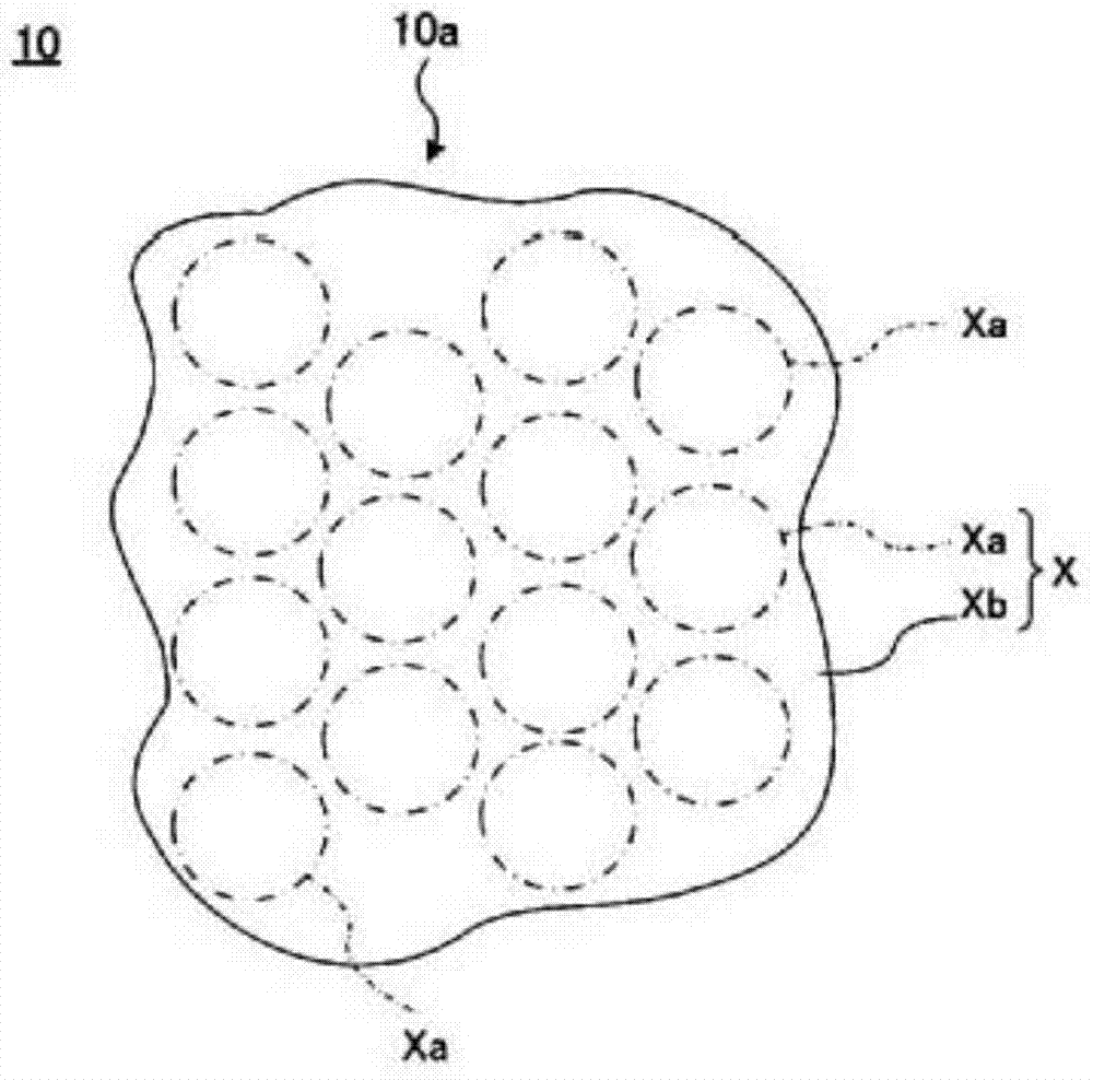
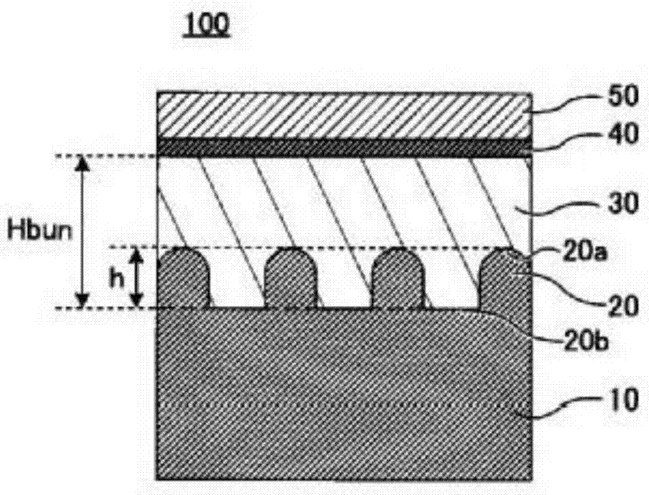
[0654] An optical substrate PP having a pattern X drawn on its surface was produced, and a semiconductor light emitting element (LED) was produced using the substrate PP, and the efficiency of the LED was compared.

[0655] In the following studies, first (1) a cylindrical master mold was fabricated, and (2) a phototransfer method was applied to the cylindrical master mold to fabricate a resin mold. (3) Next, the resin mold is processed into a sheet for nanofabrication. Next, (4) A processing mask is formed on the optical substrate using a sheet for nanofabrication, dry etching is performed through the obtained processing mask, and an optical substrate PP having a concave-convex structure PP on the surface is produced. Finally, (5) using the obtained optical substrate PP, a semiconductor light-emitting element was produced, and performance was evaluated.

[0656] (a) Production of cylindrical master mold

[0657] A fine structure is formed on the cylindr...

Embodiment 2

[0746]

[0747] An optical substrate D having a concavo-convex structure D on the surface was prepared, and a semiconductor light emitting element (LED) was fabricated using the optical substrate D, and the efficiency of the LED was compared. At this time, the arrangement or shape of the concavo-convex structure is changed and controlled (standard deviation / arithmetic mean).

[0748] In the same manner as in Example 1, (1) a cylindrical mother mold was produced, and (2) a resin mold was produced. (3) Then, using a resin mold, a member for nanofabrication (sheet for nanofabrication) is produced. Next, (4) Using the sheet for nanofabrication, a concavo-convex structure is formed on the surface of the optical substrate. Finally, (5) using the obtained optical substrate D having the concavo-convex structure D, a semiconductor light-emitting element was produced, and performance was evaluated. In addition, the (standard deviation / arithmetic mean) of the concave-convex str...

Embodiment 3

[0772]

[0773] (Production of cylindrical master mold)

[0774] As the base material of the cylindrical master mold, a cylindrical quartz glass roll with a diameter of 80 mm and a length of 50 mm was used. On the surface of this cylindrical quartz glass roll, a fine structure (fine concavo-convex structure) was formed by a direct write lithography method using a semiconductor pulse laser as follows.

[0775] First, a resist layer is formed on the fine structure of the quartz glass surface by a sputtering method. The sputtering method was performed using CuO (containing 8 atm% Si) as a target (resist layer) and with RF 100W power. The film thickness of the resist layer after film formation was 20 nm. The cylindrical mold produced as above was exposed on the following conditions while rotating at a linear velocity s=1.0 m / sec.

[0776] Semiconductor laser wavelength for exposure: 405nm

[0777] Exposure laser power: 3.5mW

[0778] X-axis pitch Px: 398nm

...


PUM


Abstract

An optical substrate PP (10) includes a substrate body and a recess / bump structure (20) formed of a plurality of bumps (20a) provided on the main surface of the substrate body. Markings (X) that can be observed with an optical microscope are formed on the main surface. The interval between the markings is larger than the pitch of the recess / bump structure (20). The markings (X) can be recognized as first areas (Xa) and a second area (Xb) by a difference in brightness in an optical microscopic image of the markings (X). A plurality of first areas (Xa) are arranged at intervals, and the second area (Xb) exists among the first areas (Xa). According to the present invention, the improvement of the internal quantum efficiency (IQE) and the improvement of the light extraction efficiency (LEE) of semiconductor light-emitting elements, which have been said to be a trade-off, are achieved at the same time.

Description

technical field [0001] The invention relates to an optical substrate, a semiconductor light-emitting element and a manufacturing method thereof. Background technique [0002] In recent years, in order to improve the efficiency of semiconductor light-emitting elements such as organic electroluminescence (OLED), phosphor, and light-emitting diode (LED), people have conducted research on improving the light extraction efficiency of semiconductor light-emitting elements. Such a semiconductor light-emitting element has a configuration in which a high-refractive-index region including a light-emitting portion is sandwiched between low-refractive-index regions. Therefore, the luminous light emitted from the light-emitting part of the semiconductor light-emitting element is a waveguide mode guided in the high-refractive-index region, is confined in the high-refractive-index region, and is absorbed into heat and attenuated during the waveguide process. As described above, in the sem...

Claims


Application Information

Patent Timeline
Patent Type & Authority Applications(China)
IPC IPC(8): H01L33/22
CPCH01L33/22H01L2933/0083H01L22/12H01L33/58H01L2933/0033H01L2933/0058
Inventor 古池润山口布士人井上直树室尾洋行
Owner ASAHI KASEI KK
Why Eureka
Try Eureka