Method for overcoming surface defect of polycrystalline silicon

A polysilicon, defect technology, applied in electrical components, semiconductor/solid-state device manufacturing, circuits, etc., can solve problems such as lattice defects, complex temperature control, cumbersome implementation process, etc., to improve service life, easy operation, and improve surface migration rate effect

Inactive Publication Date: 2015-07-22
BOE TECH GRP CO LTD +1
View PDF5 Cites 6 Cited by
  • Summary
  • Abstract
  • Description
  • Claims
  • Application Information

AI Technical Summary

Problems solved by technology

[0005] Monocrystalline silicon is formed by nucleation after laser melting. During this process, many dangling bonds and surface lattice defects are formed on the surface of polycrystalline silicon. Therefore, the quality of polycrystalline silicon must be guaranteed through subsequent hydrogen injection and dehydrogenation processes, but twice The process of process realization is cumbersome, and there are certain technical difficulties in complex temperature control

Method used


Image

  • Method for overcoming surface defect of polycrystalline silicon
  • Method for overcoming surface defect of polycrystalline silicon
  • Method for overcoming surface defect of polycrystalline silicon

Examples


Embodiment 1

[0035] This embodiment provides a method for improving polysilicon surface defects by using a sulfur-containing passivation solution, specifically as follows:

[0036] After the laser-melted polysilicon substrate is formed, slowly spray a passivation solution with a temperature of 50°C onto the surface of the substrate formed by polysilicon (the passivation solution is a saturated solution of ammonium sulfide alcohol), and the action lasts for 20 minutes to complete the surface passivation process After the surface is passivated, the residual solution on the surface of the substrate is cleaned with deionized water.

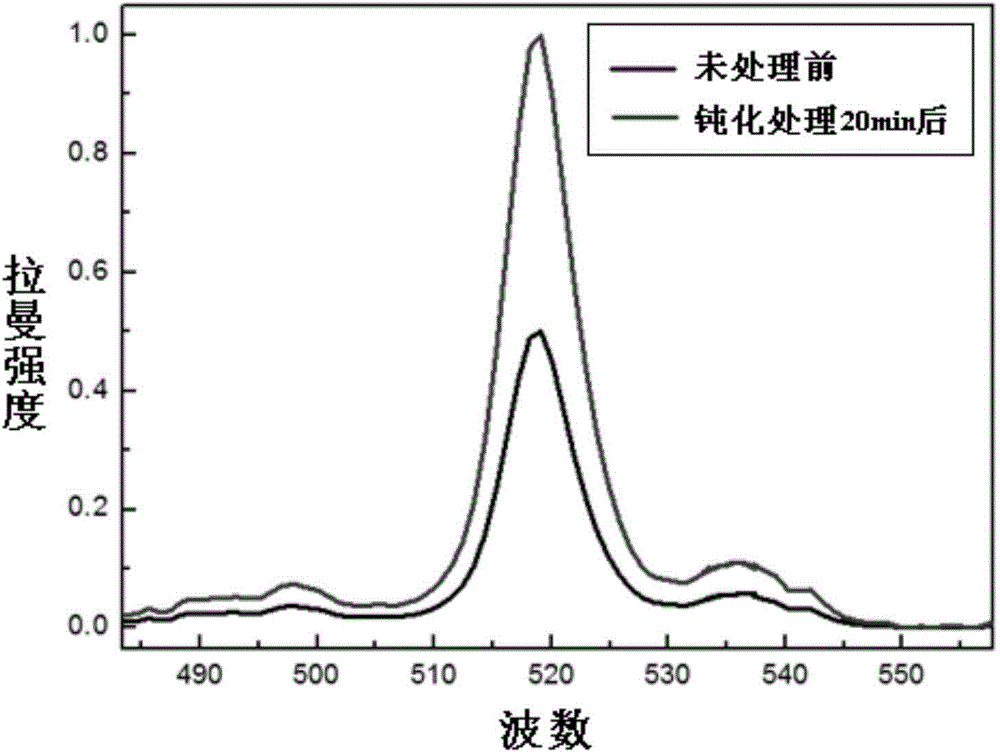
[0037] figure 1 It is a schematic diagram of the test results of polysilicon Raman spectrum after surface passivation treatment by the above method, from figure 1 The results show that the Raman spectrum intensity of the polysilicon substrate after the passivation solution treatment increases significantly, and it can be seen that the passivation solution has a g...

Embodiment 2

[0045] Compared with Example 1, the method described in this example differs only in that: in this example, the sulfur-containing passivation solution is a sodium sulfide alcohol saturated solution, its temperature is 60 ° C, and the surface passivation treatment time is 30 minutes .

Embodiment 3

[0047] Compared with the method described in Example 1, the method described in this example differs only in that the temperature of the sulfur-containing passivation solution in this example is 40° C., and the surface passivation treatment time is 10 minutes.


PUM


Abstract

The invention relates to the field of semiconductors, and particularly discloses a method for overcoming a surface defect of polycrystalline silicon. The method specifically comprises the steps that surface passivating treatment is conducted on the polycrystalline silicon through sulfur-containing passivating liquid or SCl2 gas, wherein the sulfur-containing passivating liquid is an ammonium sulfide solution or a sodium sulfide solution. According to the method for overcoming the surface defect of the polycrystalline silicon, due to the fact that surface passivating treatment is conducted on the polycrystalline silicon through the sulfur-containing passivating liquid or the SCl2 gas, the surface defect formed on the surface of the polycrystalline silicon in the polycrystalline silicon formation technological process can be effectively overcome, suspended chemical bonds can be effectively removed, the surface mobility of the polycrystalline silicon can be improved to a small extent, and the service life of the high mobility of the polycrystalline silicon can be prolonged. Compared with conventional hydrogen implantation and dehydrogenation technologies, the method has the advantages that operation is easier and more convenient, and the method can be accomplished only through the one-step technological process.

Description

technical field [0001] The invention relates to the field of semiconductors, in particular to a method for improving surface defects of polysilicon. Background technique [0002] The arrangement of atoms in materials has certain rules. For example, semiconductor materials have diamond structure, sphalerite structure, etc. The internal arrangement of atoms in each material respects certain rules. If these atoms are arranged on the surface of the material, there are faults The time is still the same as the atomic arrangement inside the material, and there are no other atoms or molecules attached to the surface material due to pollution, chemical reaction and many other reasons. This surface is an ideal surface in imagination. The distribution of electrons in the material is characterized by the wave function of the electrons. If the electron wave function of the material decays exponentially from the outside to the inside of the surface of the material, then this phenomenon sh...

Claims


Application Information

Patent Timeline
Patent Type & Authority Applications(China)
IPC IPC(8): H01L21/306
CPCH01L21/306H01L21/30604H01L21/3065
Inventor 王博玄明花
Owner BOE TECH GRP CO LTD
Why Eureka
Try Eureka