Preparation method for metal semiconductor field effect transistor with wide channel and deep recesses

A metal semiconductor and field effect transistor technology is applied in the field of preparation of metal semiconductor field effect transistors with wide channels and deep recesses, which can solve the problems of saturation current degradation, reduce drain current, lattice damage, etc. Effect

Inactive Publication Date: 2015-08-26
XIDIAN UNIV
View PDF3 Cites 5 Cited by
  • Summary
  • Abstract
  • Description
  • Claims
  • Application Information

AI Technical Summary

Problems solved by technology

[0004] Although the breakdown voltage of the double-recess structure 4H-SiC MESFET is increased due to the fact that half the length of the source side of the gate is recessed into the N-type channel layer, the saturation leakage current has not been substantially improved.
And in practice, the process of reactive i

Method used


Image

  • Preparation method for metal semiconductor field effect transistor with wide channel and deep recesses
  • Preparation method for metal semiconductor field effect transistor with wide channel and deep recesses

Examples


Embodiment 1

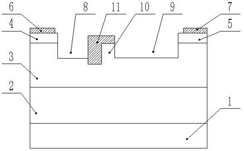
[0054] The method for fabricating a wide-channel deep-recess metal-semiconductor field-effect transistor with a thickness of 0.45 μm and a high gate region with a length of 0.35 μm and a height of 0.2 μm is as follows:

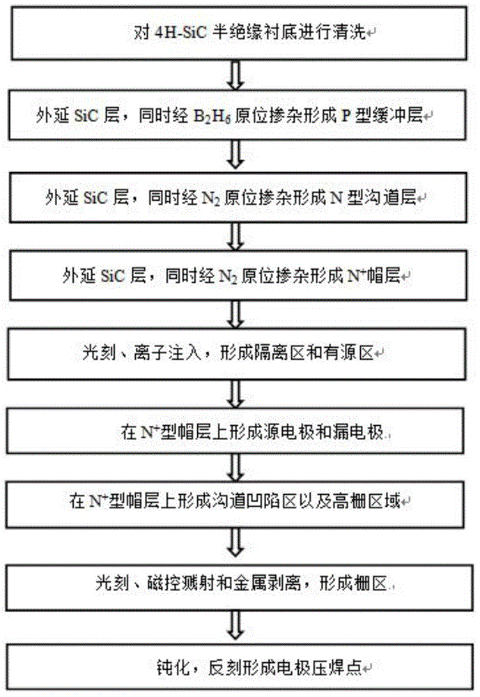
[0055] Step 1) cleaning the 4H-SiC semi-insulating substrate 1 to remove dirt on the surface of the substrate;

[0056] a. Carefully clean the substrate two or three times with a cotton ball dipped in methanol to remove SiC particles of various sizes on the surface;

[0057] b. Place 4H-SiC semi-insulating substrate 1 in H 2 SO 4 :HNO 3 = Ultrasound for 5 minutes in 1:1;

[0058] c. Put the 4H-SiC semi-insulating substrate 1 in 1# cleaning solution (NaOH:H 2 o 2 :H 2 O=1:2:5) and boiled for 5 minutes, then rinsed with deionized water for 5 minutes and then put into 2# cleaning solution (HCl:H 2 o 2 :H 2 O=1:2:7) and boiled for 5 minutes, 2# cleaning solution is HCl:H 2 o 2 :H 2 O=1:2:7, finally rinsed with deionized water and washed with N 2 Blow ...

Embodiment 2

[0090] A wide-channel deep recess metal-semiconductor field-effect transistor with a thickness of 0.4 μm and a high gate region 10 with a length of 0.35 μm and a height of 0.15 μm is fabricated. The difference between the manufacturing steps of this embodiment and Embodiment 1 is:

[0091] Step 3) epitaxially grow a 0.45 μm thick SiC layer on the P-type buffer layer 2, and at the same time 2 In-situ doping, forming a concentration of 3×10 17 cm -3 N-type channel layer 3;

[0092] The specific operation process is: put the 4H-SiC epitaxial wafer into the growth chamber, feed silane at a flow rate of 20ml / min, propane at 10ml / min and high-purity hydrogen at 80l / min into the growth chamber, and simultaneously feed 2ml / min N 2 , the growth temperature is 1550℃, the pressure is 10 5 Pa, last for 5min, complete doping concentration and thickness are 3×10 17 cm -3 and an N-type channel layer 3 of 0.4 μm.

[0093] Step 7) To the N between the source electrode 6 and the drain e...

Embodiment 3

[0098] A 4H-SiC metal-semiconductor field-effect transistor with a thickness of 0.5 μm and a high gate region 10 with a length of 0.35 μm and a height of 0.25 μm is fabricated. The difference between the manufacturing steps of this embodiment and the first embodiment is:

[0099] Step 3) epitaxially grow a 0.45 μm thick SiC layer on the P-type buffer layer 2, and at the same time 2 In-situ doping, forming a concentration of 3×10 17 cm -3 N-type channel layer 3;

[0100] The specific operation process is: put the 4H-SiC epitaxial wafer into the growth chamber, feed silane at a flow rate of 20ml / min, propane at 10ml / min and high-purity hydrogen at 80l / min into the growth chamber, and simultaneously feed 2ml / min N 2 , the growth temperature is 1550℃, the pressure is 10 5 Pa, last for 5min, complete doping concentration and thickness are 3×10 17 cm -3 and an N-type channel layer 3 of 0.5 μm.

[0101] Step 7) To the N between the source electrode 6 and the drain electrode 7...


PUM

PropertyMeasurementUnit
Thicknessaaaaaaaaaa
Thicknessaaaaaaaaaa
Lengthaaaaaaaaaa

Abstract

The invention belongs to the technical field of field effect transistors, and particularly discloses a preparation method for a metal semiconductor field effect transistor with wide channels and deep recesses. The preparation method for the metal semiconductor field effect transistor with the wide channels and deep recesses settles the problems in prior art and has advantages of realizing simple manufacture process, enlarging an output current and a breakdown voltage, and improving frequency characteristic. The preparation method comprises the steps of cleaning a semi-insulating substrate; realizing epitaxial growth of a P-type buffer layer; realizing epitaxial growth of an N-type channel layer on the P-type buffer layer; realizing epitaxial growth of an N<+> cap layer on the N-type channel layer; preparing an isolation region and an active region; preparing a source electrode and a drain electrode; performing lithography and etching on the N<+> between the source electrode and the drain electrode, thereby forming a high-gate area; manufacturing a gate electrode; and manufacturing an electrode pads, thereby finishing device preparation.

Description

Technical field: [0001] The invention belongs to the technical field of field effect transistors, in particular to a preparation method of a metal semiconductor field effect transistor with a wide channel and a deep recess. Background technique: [0002] SiC materials have outstanding material and electrical properties such as wide band gap, high breakdown electric field, high saturated electron migration velocity, and high thermal conductivity, making them suitable for high-frequency and high-power device applications, especially high temperature, high voltage, aerospace, satellite, etc. It has great potential in high-frequency high-power device applications in harsh environments. In SiC allomorphs, the electron mobility of 4H-SiC with hexagonal close-packed wurtzite structure is nearly three times that of 6H-SiC, so 4H-SiC materials are used in high-frequency and high-power devices, especially in metal-semiconductor fields. Effect transistor (MESFET) occupies a major posi...

Claims


Application Information

Patent Timeline
IPC IPC(8): H01L21/336
CPCH01L29/66477
Inventor 贾护军张航邢鼎杨银堂
Owner XIDIAN UNIV
Why Eureka
Try Eureka