Method for manufacturing silicon carbide high-temperature ion implantation mask with selectivity cut-off layer

A technology of high-temperature ion implantation and manufacturing method, which is applied in the manufacture of semiconductor/solid-state devices, electrical components, circuits, etc. Good control and other issues to avoid contamination on the surface of the device, simplify the surface cleaning process, and achieve the effect of good blocking effect

Active Publication Date: 2014-02-12
江苏中科汉韵半导体有限公司
View PDF6 Cites 4 Cited by
  • Summary
  • Abstract
  • Description
  • Claims
  • Application Information

AI Technical Summary

Problems solved by technology

This method is not only complicated in process, but also the formed ion implanted sacrificial layer film is affected by the thick medium ion implanted mask layer, which has poor in-plane uniformity and controllability, which seriously affects the doping distribution of the selective ion implanted region, thus affecting The breakdown characteristics of the device; 2) The ion implantation sacrificial layer is first formed by thermal oxidation, and then the high temperature ion implantation masking layer is deposited, and etched to the surface of the ion implantation sacrificial layer by etching
This method is feasible, but the etching technology is not easy to control
The wet etching rate is slow, and the etching is isotropic, and it is difficult to form a steep etching sidewall
Dry etching, usually using ICP etching, can form steep sidewalls, but because the ion implantation sacrificial layer is very thin, and the etching selectivity ratio to the masking layer is not high, over-etching is easy to occur during the etching process Corrosion phenomenon, causing damage to the device surface

Method used


Image

  • Method for manufacturing silicon carbide high-temperature ion implantation mask with selectivity cut-off layer
  • Method for manufacturing silicon carbide high-temperature ion implantation mask with selectivity cut-off layer
  • Method for manufacturing silicon carbide high-temperature ion implantation mask with selectivity cut-off layer

Examples


Embodiment

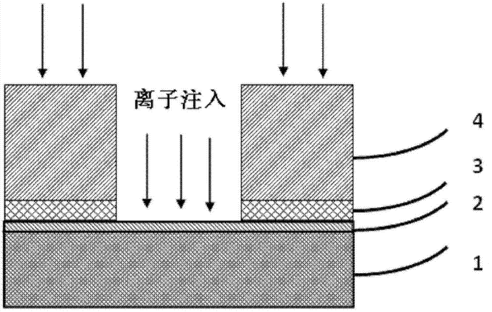
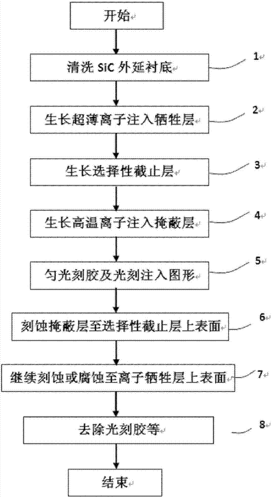
[0043] In order to understand the present invention in depth, the present invention will be described in detail below in conjunction with specific embodiments, a method for forming a silicon carbide high-temperature ion implantation mask with a selective cut-off layer on a silicon carbide (SiC) epitaxial substrate:

[0044] Step 1: Clean the silicon carbide substrate with standard RCA (3#, 1# each for 10 minutes), and clean it with N 2 Blow dry chips.

[0045] Step 2: On the clean silicon carbide substrate obtained in the previous step, grow a 20-30nm ion-implanted sacrificial layer film at 1150° C. for 90 minutes by using wet oxygen (hydrogen-oxygen ignition) method.

[0046] Step 3: growing a 500 angstrom amorphous silicon layer at 550° C. as a selective cut-off layer on the ion-implanted sacrificial layer film obtained in the previous step by LPCVD.

[0047] Step 4: On the basis of the previous step, use the PECVD growth method to grow 2μm SiO on the amorphous silicon laye...


PUM


Abstract

The invention discloses a method for manufacturing a silicon carbide high-temperature ion implantation mask with a selectivity cut-off layer. The method includes the steps of cleaning a silicon carbide substrate, adopting a heat oxidation method to grow an ion implantation sacrificial layer mask on the silicon carbide substrate, adopting an LPCVD method to grow the selectivity cut-off layer used for controlling the etching process on the obtained ion implantation sacrificial layer mask, adopting an epitaxy or growing method to form an insulating medium masking layer on the selectivity cut-off layer, evenly coating the insulating medium masking layer with photoresist, carrying out photoetching to develop a selectivity ion implementation area window, carrying out dry-method etching or corrosion on the insulating medium masking layer from the selectivity ion implementation area window to the surface of the selectivity cut-off layer, continuously carrying out etching or corrosion to the surface of an ion implantation sacrificial layer, removing the photoresist, and obtaining the ultra-thin ion implementation sacrificial layer mask. The method for manufacturing the silicon carbide high-temperature ion implantation mask is suitable for a silicon carbide SBD, a JBS diode, an MOSFET device and other silicon carbide devices requiring high-temperature high-energy ion implantation.

Description

technical field [0001] The invention relates to the fields of ion implantation mask preparation technology and etching / corrosion technology, in particular to a method for manufacturing a silicon carbide (SiC) high temperature ion implantation mask with a selective cut-off layer. Background technique [0002] Silicon carbide material has excellent physical and electrical properties. With its unique advantages such as wide band gap, high thermal conductivity, large saturation drift velocity and high critical breakdown electric field, it has become a high-power, high-frequency, durable It is an ideal semiconductor material for high-temperature and radiation-resistant devices, and has broad application prospects in military and civil affairs. Power electronic devices made of SiC materials have become one of the hot devices and frontier research fields in the field of semiconductors. [0003] Mask technology is one of the important processes in semiconductor manufacturing, and i...

Claims


Application Information

Patent Timeline
Patent Type & Authority Applications(China)
IPC IPC(8): H01L21/266
CPCH01L21/266
Inventor 刘新宇许恒宇汤益丹蒋浩杰赵玉印申华军白云杨谦
Owner 江苏中科汉韵半导体有限公司
Why Eureka
Try Eureka