

Silicon carbide avalanche photodiode with novel small-dip-angle half mesa structure
A mesa structure, avalanche photoelectric technology, applied in circuits, electrical components, semiconductor devices, etc., can solve the problems of waste of chip area and low filling factor, and achieve the effect of increasing the effective area of the chip, increasing the filling factor, and reducing the length.
- Summary
- Abstract
- Description
- Claims
- Application Information
AI Technical Summary
Problems solved by technology
Method used
Image

Examples
Embodiment 1
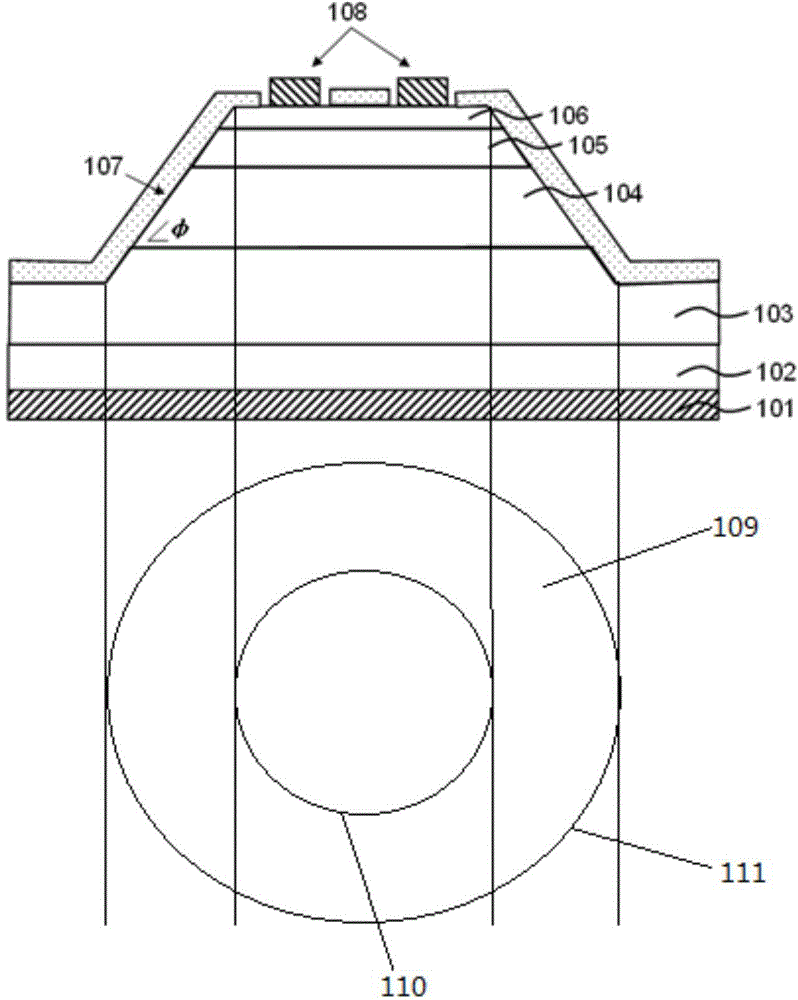
[0039] Such as image 3 As shown, the small-tilt half-mesa SiC APD structure is fabricated on an n-type conductive SiC substrate. From the bottom to the top of the n-type conductive SiC substrate 102 are the n-type SiC contact layer 103, the i-type SiC avalanche layer 104, the p-type SiC transition layer 105, and the p+-type SiC contact layer 106; It only needs to be etched below the p-type SiC transition layer 105 , and the bottom of the mesa is on the i-type SiC avalanche layer 104 .
Embodiment 2
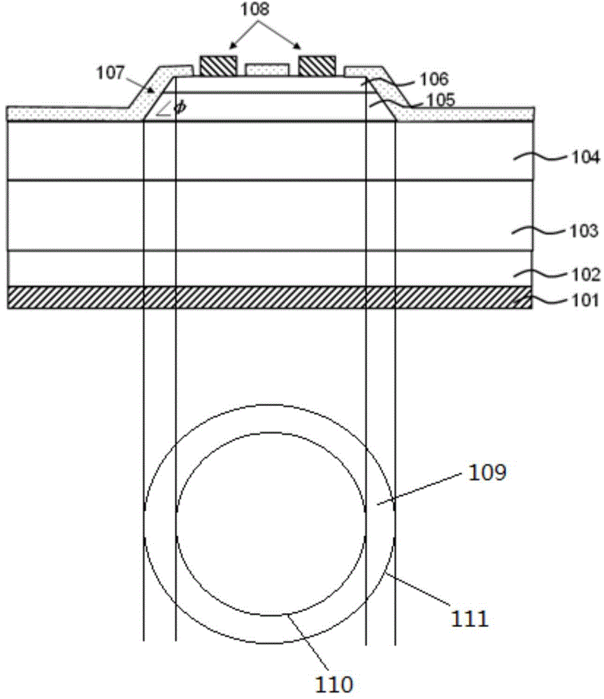
[0053] Figure 6 It is a schematic structural diagram of another small-tilt half-mesa SiC APD device proposed by the present invention, which is prepared on a p-type conductive SiC substrate material. Figure 6 The device structure shown with the image 3 The device structure shown has a symmetrical relationship in which the conduction polarities of the SiC material are just opposite from top to bottom. The basic components of the device include: a p-type conductive SiC substrate 202 with a doping concentration greater than 1×10 17 cm -3 . On the p-type conductive SiC substrate 202, a p-type SiC contact layer 105, an i-type SiC avalanche layer 104, an n-type SiC transition layer 103, and an n+-type SiC ohmic contact layer 206 are sequentially grown; wherein, the p-type SiC contact layer 105 The average doping concentration should be between 1×10 17 -1×10 20 cm -3 Between, the thickness is between 0-50 μm; the average doping concentration of the i-type SiC avalanche laye...
PUM
| Property | Measurement | Unit |
|---|---|---|
| Bottom corner | aaaaa | aaaaa |
| Thickness | aaaaa | aaaaa |
| Thickness | aaaaa | aaaaa |
Abstract
Description
Claims
Application Information