Bridge type input resistance negative feedback CMOS (Complementary Metal Oxide Semiconductor) pre-amplifying circuit

A technology of input resistance and pre-amplification circuit, which is applied in the field of CMOS circuits, can solve the problems of easy interference and mismatch of signals, and achieve the effect of benefiting equivalent input noise and reducing equivalent input noise

Inactive Publication Date: 2015-09-02
SHANGHAI INST OF TECHNICAL PHYSICS - CHINESE ACAD OF SCI
View PDF6 Cites 1 Cited by
  • Summary
  • Abstract
  • Description
  • Claims
  • Application Information

AI Technical Summary

Problems solved by technology

[0004] The present invention proposes a CMOS pre-amplifier circuit, which adopts a bridge input mode in the input part, which overcomes the problem that the existing CMOS circuit does not match the low-impedance detector, and the circuit is suitable for low-impedance detector signals below 100 ohms. Amplification can also work normally at the low temperature of liquid nitrogen, so that the CMOS pre-amplifier circuit and the detector can work normally at the low temperature of liquid nitrogen after interconnection, which overcomes the fact that the current detector works at low temperature and the circuit works at normal temperature , the disadvantage that the signal is extremely easy to cause interference during transmission

Method used


Image

  • Bridge type input resistance negative feedback CMOS (Complementary Metal Oxide Semiconductor) pre-amplifying circuit
  • Bridge type input resistance negative feedback CMOS (Complementary Metal Oxide Semiconductor) pre-amplifying circuit
  • Bridge type input resistance negative feedback CMOS (Complementary Metal Oxide Semiconductor) pre-amplifying circuit

Examples


Embodiment 1

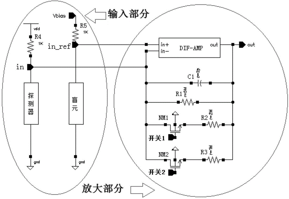
[0019] figure 1 The overall structure diagram of the CMOS preamplifier circuit for negative feedback of the bridge input resistance. R4 is connected with the infrared photoconductive detector to form a path, R5 is connected with the blind element of the detector to form another path, and the two paths form a balanced bridge structure. If you want to increase or decrease the current flowing through the photoconductive detector, you can increase or decrease the resistance of R4 and R5. R5 corresponds to R4, and its resistance should be designed to be equal, and the design of this circuit is 1K ohms. The resistance of the blind element and the detector are equal in size. If the resistance of the detector is inconsistent with the resistance of the blind element, the circuit can work normally by adjusting Vbias. The amplifier is suitable for amplifying signals of photoconductive detectors with low input impedance below 100 ohms. When the infrared photoconductive detector receive...

Embodiment 2

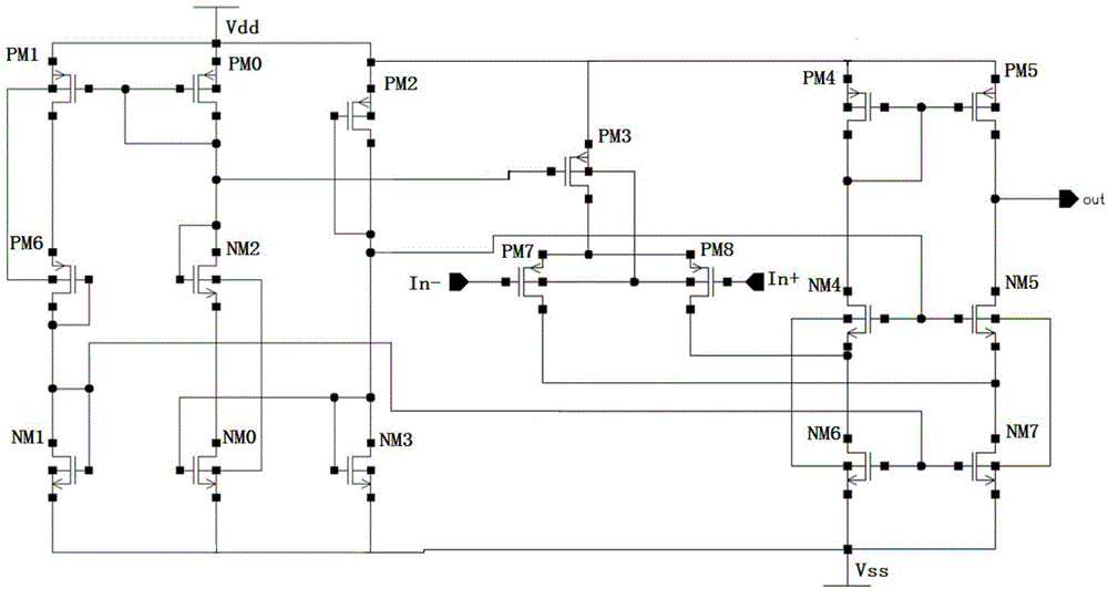
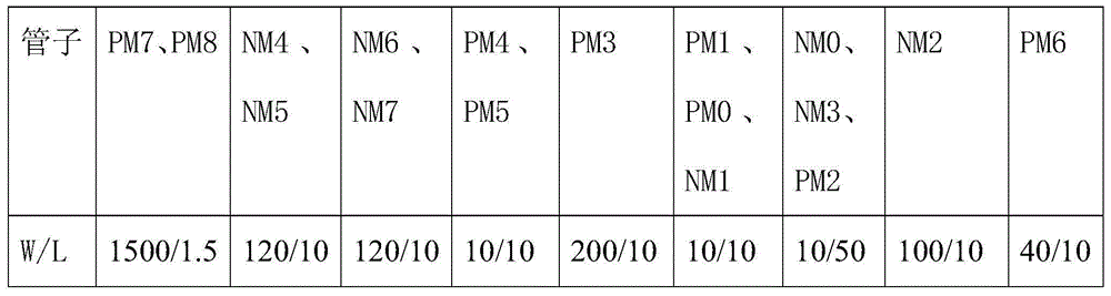
[0023] figure 2 It is the topological structure diagram of the differential amplifier circuit. One-stage folded cascode structure with differential input. Among them, PM7 and PM8 are input pair tubes, PM7, PM8, NM4, and NM5 form a cascode structure of differential input, PM4, PM5 are active loads of differential output, NM6, NM7 provide current source for cascode, In -, In+ are the positive and negative input terminals of the differential operational amplifier. NM3 and NM0 constitute the first-stage current mirror, PM0 and PM1 constitute the second-stage current mirror, NM1 and NM6 and NM7 of the amplifying part constitute a current mirror, and PM0 and PM3 of the amplifying part constitute a current mirror. The reference dimensions of the tubes are shown in the table below (in microns).

[0024]

[0025] The differential amplifier adopts a cascode structure and can be powered by positive and negative power sources, so that there is no minimum voltage requirement at the ...

Embodiment 3

[0027] Under the low temperature of liquid nitrogen, the CMOS preamplifier circuit was tested, and its minimum amplification factor was 400 times (0.6M ohm feedback resistance). Then the CMOS preamplifier circuit was interconnected with the low-impedance detector, and the component was tested. The working condition of the circuit and the detector is good. The 3dB bandwidth of the component is greater than 2KHZ, and the noise of the equivalent input point is less than 30nV / Hz -1 / 2 . The passband noise was tested with a lock-in amplifier EG Model 117, and the results are shown in the table below:

[0028]

[0029] From the test results, the bridge-type input resistance negative feedback CMOS preamplifier circuit can be read out smoothly after the low-impedance detector is connected to the low-temperature liquid nitrogen, and the noise test results are excellent, successfully realizing the high-impedance CMOS circuit and low-impedance detector matching.


PUM


Abstract

The invention discloses a bridge type input resistance negative feedback CMOS (Complementary Metal Oxide Semiconductor) pre-amplifying circuit, which consists of an input part and an amplification part, wherein the input part is directly coupled with the amplification part. According to the circuit, a balance bridge type input structure is adopted for the input part, 1 kilo-ohm bias resistance is adopted for each of two branch circuits of the input part, one branch circuit is connected with a detector to form a path, the other branch circuit is connected with a blind pixel to form another path, and the two paths form the balance bridge type input structure; in order to meet the requirements of different amplification factors and achieve adaptability to the amplification readout of detector signals with different response ratios, a variable gain resistance negative feedback structure is adopted for the amplification part, selectable 5, 2 or 1 meg-ohm feedback resistance is adopted between the negative input end and the output end of the amplification part, and feedback resistances with different magnitudes are formed under the control of two MOS switches; in order to enable the circuit to work at low temperature of liquid nitrogen, a common-source common-gate structure is adopted for a differential amplifier in the amplification part, and the differential amplifier is powered by positive and negative power supplies.

Description

technical field [0001] The invention relates to a CMOS circuit, in particular to a CMOS pre-amplifier circuit with negative feedback of a bridge input resistance. Background technique [0002] In the field of aerospace remote sensing, infrared detector components are the core components of infrared imaging systems. Because photoconductive infrared detectors have great advantages in the long-wave field, most long-wave infrared detection uses photoconductive infrared detectors. The internal resistance is very low, generally lower than 100 ohms, and it works at the low temperature of liquid nitrogen, which puts forward higher requirements for the circuit interconnected with this type of detector. Work in liquid nitrogen cryogenics. At present, most of the long-wave photoconductive infrared detector signal readout adopts the design method of separating the detector and the circuit. The detector works at low temperature, and the circuit works at normal temperature. The signal is...

Claims


Application Information

Patent Timeline
Patent Type & Authority Applications(China)
IPC IPC(8): H03F1/34H03F3/45
Inventor 袁红辉陈世军陈永平
Owner SHANGHAI INST OF TECHNICAL PHYSICS - CHINESE ACAD OF SCI
Why Eureka
Try Eureka