Ga40Sb60/Sb superlattice phase transition film material for high-speed low-power-consumption phase change memory, and preparing method thereof

A phase-change memory and thin-film material technology, applied in the field of microelectronics, can solve problems such as unsatisfactory data retention, and achieve the effects of small changes in the overall structure, improved stability and reliability, and accelerated phase transition speed.

Active Publication Date: 2015-09-09
JIANGSU UNIV OF TECH
View PDF8 Cites 14 Cited by
  • Summary
  • Abstract
  • Description
  • Claims
  • Application Information

AI Technical Summary

Problems solved by technology

However, there are certain contradictions between the above characteristics, for example, faster crystallization speed usually means lower crystallization temperature, and lower crystallization temperature usually leads to unsatisfactory data retention
Therefore, the biggest challenge in research work is to find an optimal and balanced result

Method used


Image

  • Ga40Sb60/Sb superlattice phase transition film material for high-speed low-power-consumption phase change memory, and preparing method thereof

Examples


Embodiment 1)

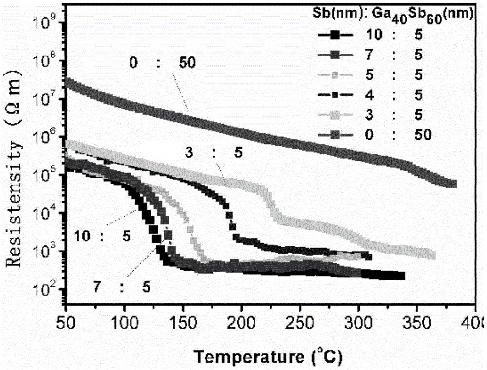
[0027] Ga 40 Sb 60 / Sb superlattice phase change film material is a multilayer composite film structure with a thickness of 6-80nm; made of Ga 40 Sb 60 Layers and Sb layers are alternately deposited and compounded, that is, in thin films, according to Ga 40 Sb 60 Layer - Sb Layer - Ga 40 Sb 60 The sequence of layer-Sb layer... is repeated alternately.

[0028] A layer of Ga 40 Sb 60 layer and a layer of Sb as an alternating period, the latter alternating period of Ga 40 Sb 60 layer deposited on top of the Sb layer of the previous alternate period. Ga 40 Sb 60 The layer contains two elements, Ga and Sb, and the atomic ratio of Ga and Sb is 4:6.

[0029] The above Ga 40 Sb 60 The general formula [Ga 40 Sb 60 (a) / Sb(b)] x Indicates that a is a monolayer Ga 40 Sb 60 The thickness of the layer, 1nm≤a≤50nm; b is the thickness of the single-layer Sb layer, 1nm≤b≤50nm; x is Ga 40 Sb 60 layer and the number of alternating periods of the Sb layer, or a layer of Ga...

Embodiment 2)

[0043] Ga 40 Sb 60 The film structure of the Sb-like superlattice phase change film material is [Ga 40 Sb 60 (5nm) / Sb(7nm)] 4 , that is, each layer of Ga 40 Sb 60 The thickness of the layer is 5nm, the thickness of each layer of Sb is 7nm, Ga 40 Sb 60 layer and Sb layer alternate period number is 4, Ga 40 Sb 60 The thickness of the / Sb-type superlattice phase-change thin film material is 48nm.

[0044] The rest of the preparation method are the same as in Example 1, the difference is: step 3. magnetron sputtering prepares Ga 40 Sb 60 / Sb superlattice phase change thin film material, the sputtering time of each layer of Sb is 21s.

Embodiment 3)

[0046] Ga 40 Sb 60 The film structure of the Sb-like superlattice phase change film material is [Ga 40 Sb 60 (5nm) / Sb(5nm)] 5 , that is, each layer of Ga 40 Sb 60 The thickness of the layer is 5nm, the thickness of each layer of Sb is 5nm, Ga 40 Sb 60 layer and Sb layer alternate period number is 5, Ga 40 Sb 60 The thickness of the / Sb superlattice phase change film material is 50nm.

[0047] The rest of the preparation method are the same as in Example 1, the difference is: step 3. magnetron sputtering prepares Ga 40 Sb 60 / Sb superlattice phase change thin film material, the sputtering time of each layer of Sb layer is 15s.


PUM

PropertyMeasurementUnit
thicknessaaaaaaaaaa
thicknessaaaaaaaaaa
thicknessaaaaaaaaaa

Abstract

The invention discloses a Ga40Sb60 / Sb superlattice phase transition film material for high-speed low-power-consumption phase change memory. The Ga40Sb60 / Sb superlattice phase transition film material has a multilayer composite film structure and is obtained through alternately depositing Ga40Sb60 layers and Sb layers. One Ga40Sb60 layer and one Sb layer are used as one alternating period, and the Ga40Sb60 layer of the next alternating period is deposited on the Sb layer of a previous alternating period. According to the Ga40Sb60 / Sb superlattice phase transition film material, a clamping effect of a multilayer interface in a superlattice structure is utilized for reducing dimensions of crystal particles, thereby shortening crystallization time, restraining crystallization, improving thermal conductivity of the material and furthermore increasing phase change speed. Furthermore the Ga40Sb60 / Sb superlattice phase transition film material has advantages of realizing small size change in the phase change process, ensuring good contact between a phase change layer and electrode material, and finally improving stability and reliability of a phase change memory device.

Description

technical field [0001] The invention relates to the field of microelectronic technology, in particular to a Ga 40 Sb 60 / Sb-type superlattice phase-change thin film material and preparation method thereof. Background technique [0002] The 21st century is the information age of globalization, and information is playing an increasingly important role in human life. The recording and preservation of information is the storage of information, so information storage technology is one of the supporting technologies in the information age. In recent years, in order to solve the problems faced by traditional storage technologies such as flash memory (FLASH) technology, dynamic memory (DRAM) and static memory (SRAM), many semiconductor manufacturers and research institutions are working hard to develop a new generation of non-volatile memory. Among them, Phase Change Random Access Memory (Phase Change Random Access Memory, abbreviated as PCRAM) has a long cycle life (>10 13...

Claims


Application Information

Patent Timeline
Patent Type & Authority Applications(China)
IPC IPC(8): H01L45/00C23C14/35
Inventor 邹华胡益丰朱小芹眭永兴郑龙吴卫华吴世臣袁丽薛建忠张剑豪
Owner JIANGSU UNIV OF TECH
Why Eureka
Try Eureka